Facebook
 Google
 GitHub
 Linkedin
Robustness of SiC JFETs and Cascodes
This article sheds light on the short-circuit and avalanche behavior of the standalone JFET, and how it is altered in the cascode implementation
United Silicon Carbide supplies a SiC vertical trench normally-on JFET, which features the lowest specific on-resistance of any 1200V power device. This article sheds light on the short-circuit and avalanche behavior of the standalone JFET, and how it is altered in the cascode implementation.
Trench JFET Structure
Figure 1 shows the structure of the trench JFET. The low on-resistance derives from the vertical channel that repeats with a high cell density, creating a short path between the source and drain contacts via the channel and drift regions. The drift region doping and thickness are set by the desired voltage rating. This device does not contain a body diode or any parasitic NPN transistor. It does not have a gate-oxide or any surface conduction path.
A junction diode is formed as shown be-tween the gate-source and the gate-drain regions. A normally-on JFET typically has a -6V threshold. To achieve full blocking capability up to 1200V, usually a reverse bias VGS of -15V to -20V is applied between the gate and source. This depletes the channel region, forming a potential barrier between the drain and source. If a high drain voltage is now applied, the device will block this volt-age by depleting the drift region.
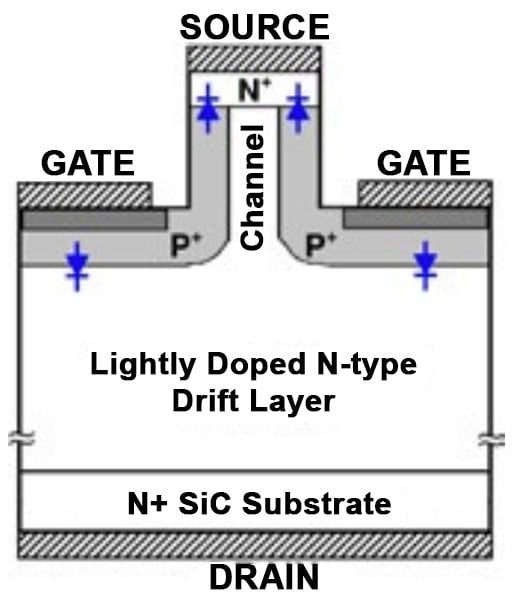
Figure 1: Cell structure of SiC trench
In the on-state, if the gate-source potential is 0V, the channel region is undepleted. A low resistance current path is seen to exist directly from the source to the drain. As this current rises, the potential at the drain side of the channel increases. When this potential at the drain side of the channel reaches the 6V threshold, the channel pinches off and the current saturates.
Figure 2 presents the typical on-state characteristics of 1200V-80mΩ SiC normally-on JFETs at different junction temperatures, showing the rapid decrease in saturation cur-rent with junction temperature. This occurs because of increase scattering of electrons at higher temperatures driven by greater lattice vibrations in the SiC crystal that in turn leads to a drop in electron mobility.

Figure 2: Typical on-state characteristics of 1200V-80mΩ SiC normally-on JFETs.
Co-packaged Cascode Structure
The normally-off operation mode can be implemented by connecting a normally-on JFET and a low-voltage normally-off MOSFET in a cascode configuration. The cascode can be constructed with a stacking structure [1], a side-by-side co-packaged structure, or a discrete structure [2]. Figure 3a shows the structure of the co-packaged cascode, where a customized Silicon low voltage MOSFET is connected in series with a SiC normally-on JFET to implement a normally-off device. The equivalent circuit is shown in Figure 3b. Figure 4 shows the typical on-state characteristics of 1200V-60mΩ SiC co-packaged cascode. The cascode device has a threshold voltage (VTH) of 4.5V and is fully enhanced for the gate voltage (VGS) values above 10V.
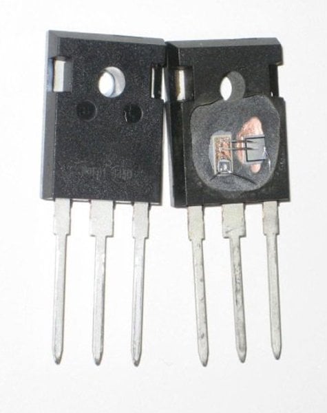
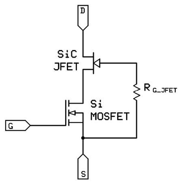
Figure 3: Co-packaged SiC cascode in TO-247 package (a) and equivalent circuit (b)
The cascode is turned on by turning on the low voltage MOSFET. Since the MOSFET drain-source voltage drop is small (ID*RDSON), the JFET gate-source voltage is near zero during on-state and the JFET channel can conduct.
When the low voltage MOSFET is turned off, the drain potential rises. The MOSFET VDS appears as a negative VGS on the SiC JFET, turning it off.
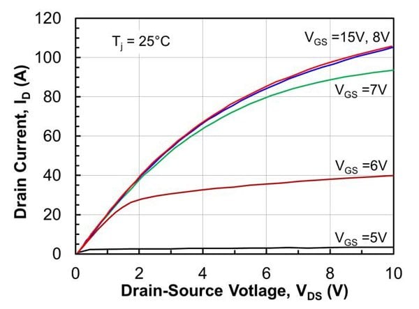
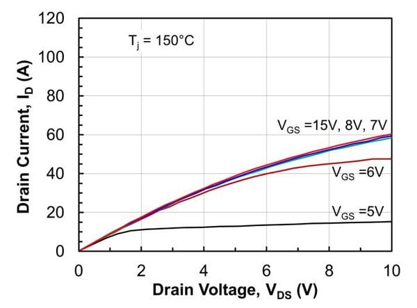
Figure 4: Typical on-state characteristics of 1200V-‐60mΩ co-‐packaged SiC cascode at a junction temperature of 25°C (a) and 150°C (b).
JFET and Cascode in Short Circuit
Figure 5 shows the short circuit waveform of the 1200V-80mΩ, SiC normally-on JFET taken at 600V bus voltage, 25°C initial junction temperature, and 0V gate-source voltage. The peak short-circuit current of the JFET depends on the cell density and threshold voltage. More negative threshold voltage translates to higher peak short circuit current. This is equivalent to higher short circuit currents with higher gate voltages on IGBTs. The short circuit withstand time depends on the peak current, and the device is shown surviving a 10µs pulse in Figure 5. As with IGBTs, there is a trade-off between short circuit capability and on-resistance/turn-on speed.
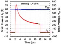
Figure 5: Measured short-circuit waveforms of a 1.2kV-80mΩ SiC normally-ON JFET at a starting Tj of 25°C and a bus voltage of 600V.
Rapid self-heating during short circuit causes the channel conductivity to decrease, and the short circuit current decreases. This negative feedback mechanism also ensures that short circuit current flow in the device is uniform. The die size of SiC JFETs is quite small, given the excellent on-resistance per unit area. The temperature rise is quite high during short-circuit, but since the intrinsic temperature of SiC is so much higher than Silicon, and because the trench JFET lacks a parasitic bipolar structure, it has excellent short circuit robustness.
Figure 6 shows the 600V 10µs short circuit waveforms of the cascode at various gate voltages. The Silicon LV MOSFET is chosen with a much higher saturation current than the JFET, so the JFET sets the saturation current, and therefore, the short circuit withstand time. The designer can choose the LV MOSFET gate voltage without worrying about the short circuit trade-off. During this event, the power dissipated in the Silicon MOSFET is quite small and does not limit the cascode short-circuit capability.
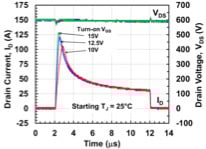
Figure 6: Measured short-circuit waveforms of a 1.2kV-100mΩ SiC cascode at a starting Tj of 25°C and a bus voltage of 600V.
JFET and Cascode Avalanche Behavior Figure 7 shows the blocking characteristics of 1200V-80mΩ SiC normally-on JFET. It is apparent that beyond a gate voltage VGS of -15V the device goes into avalanche breakdown. Figure 8 shows the measured un-clamped inductive switching (UIS) waveform of a 1200V-60mΩ standalone JFET, along with the schematic of the circuit used for the measurement [3].

Figure 7: Blocking characteristics of 1200V- 80mW SiC normally-ON JFETs at room temperature.
The peak current is 25.5A, the avalanche time tav is 23.7µs, and the energy dissipated in the JFET is 489.1mJ obtained from the integration of the instant power (Vds x Iav) over the entire avalanche period. The device has no change in its characteristics before and after the UIS testing, proving its UIS robustness. Once the device is driven into avalanche, current initially flows in the gate-drain diode of the JFET. It develops voltage across the internal Rg and external Rg. This causes the gate potential to rise, until it eventually crosses the -6V threshold voltage of the JFET. The channel gets turned-on (in saturation mode, since the drain voltage is still high) to handle all the rest of the drain current. This can be seen from the plateau in the gate voltage VGS waveform in Figure 8. So, a considerable fraction of the current during unclamped inductive switching is actually diverted to the channel, rather like a MOSFET used with an active clamp.
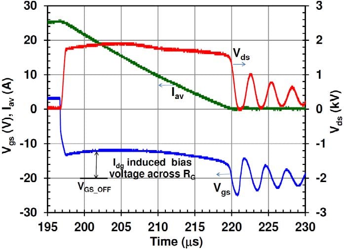

Figure 8: Measured unclamped inductive switching waveforms of a 1200V-60mΩ standalone SiC normally-ON JFET at a starting junction temperature of of 25°C with a 1.5mH inductor (a) and the schematic of the testing circuit (b)
The high current and voltage during this type of high energy avalanche stress leads to considerable temperature rise in the JFET. Since the JFET has no parasitic bipolar structure, and because the intrinsic temperature of SiC is so much higher than Silicon, excellent avalanche capability can be obtained even with the small SiC die sizes.
USCI JFETs are 100% avalanche tested at final test. During device development, tests are done to ensure 106 cycles of UIS can be passed by all sampled devices.
Figure 9 shows the measured unclamped inductive switching waveform of a 1.2kV SiC cascode [2]. The cascode avalanche capability is found to be quite similar to that of the JFET, and is not limited by the LV Silicon MOSFET. Once the LV MOSFET is turned off, and the SiC JFET drain voltage rises to its avalanche breakdown level, current flows initially in the gate-drain diode. Again, it develops a voltage across the internal RG of the JFET. This voltage reaches BV(LV MOS) – VTH(JFET). At that current, the JFET channel is again turned on, and the rest of the UIS current flows through the channel as before. Again, the gate-drain diode takes some of the avalanche current, depending on the current level, and the channel handles the rest. In this mode, the LV MOSFET is also driven to avalanche, carrying the same current as the SiC JFET channel region. The LV MOSFET is specially designed with a built-in avalanche clamp diode in every cell. Due to its low breakdown voltage, the energy dissipated in the low voltage FET does not cause a large temperature rise at the current levels used for the cascode.

Figure 9: Measured UIS waveforms without failure of a 1.2kV SiC cascode at a starting Tj of 25°C and an inductor of 1.5mH.
Note that if the internal RG of the JFET was zero, and the JFET gate was shorted to the source of the LV MOSFET, all of the avalanche current would flow in the gate-drain diode of the SiC JFET, which is simply a Drain-Source current path in the cascode. The SiC JFET can handle this mode of operation as well, but some gate resistance is built into the cascode to limit its maximum switching speed.
As with the JFETs, USCI Cascodes are 100% avalanche tested at final test. During device development, tests are done to ensure 106 cycles of UIS can be passed by all sampled devices. In addition, the LV MOSFET is qualified by burn-in with the device biased into avalanche for 1000hrs at a junction temperature of 150°C.
Summary
SiC JFETs and Cascodes have excellent short circuit and avalanche capability. The reasons for this behavior are explained in the article. Consideration was given during the design of the SiC JFETs and cascodes to ensure that the devices are capable of handling repetitive avalanche events within their SOA, like most Silicon MOSFETs. The peak temperatures handled by SiC devices on the micro-second scale can be 2-3X higher than for Silicon devices, and this is why good avalanche and short circuit ratings can be realized despite the small die sizes.
About the Author
Anup Bhalla works as the Vice President of Engineering at United Silicon Carbide, Inc. where he is responsible for commercializing SiC-based Diodes, trench vertical JFETs, BJTs, trench vertical MOSFETs, GTOs and ICs. He earned his Bachelor's Degree in Electrical Engineering at the Indian Institute of Technology. He also holds a Master's Degree and Doctorate Degree in Electrical Engineering both earned at the Rensselaer Polytechnic University.
John Bendel works as the Senior Director for Business Marketing at United Silicon Carbide, Inc. since May 2014 where he is skilled in the field of semiconductors and power management. He earned his Bachelor's Degree in Electrical Engineering at the University of California, Davis.
Xueqing Li received the B.S. degree in electrical engineering from Tsinghua University, Beijing, China, in 1990, the M.S. degree in physical electronics and optoelectronics from the Institute of Electronics, Chinese Academy of Sciences, Beijing, in 1993, and the PhD degree in electrical and computer engineering from Rutgers University, Piscataway, NJ, in 2005. Since 2003, he has been a Senior Research Engineer with United Silicon Carbide, Inc., New Brunswick, NJ, where he is responsible for the design and simulation of power devices in 4H-SiC, creation of PSpice model of power semiconductor devices, and simulation of switching-mode power converter systems.
References
- Li, Xueqing; Alexandrov, Petre; Hostetler, John; and Bhalla, Anup, “Evaluation of SiC Stack Cascode for 200°C Operation,” Materials Science Forum, vol. 778- 780, 2014, pp.879-882.
- Li, Xueqing; Bhalla, Anup; Alexandrov, Petre; Hostetler, John; and Fursin, Leonid, “Investigation of SiC Stack and Discrete Cascodes,” Proceedings of PCIM Europe 2014 , May 20-22, 2014, Nuremberg, Germany.
- Li, Xueqing; Bhalla, Anup; Alexandrov,Petre; and Fursin, Leonid, “Study of SiC Vertical JFET Behavior during Unclamped Inductive Switching,” APEC 2014, March 16-20, 2014, Fort Worth, TX, pp.2588 - 2592