Facebook
 Google
 GitHub
 Linkedin
Switching Behavior of USCis SiC Cascodes
This article examines the hard switching turn-on and turn-off mechanisms in this device, to give the users some insight the difference of MOSFETs and IGBT.
The co-packaged cascode device, combining a Silicon low voltage FET with a trench vertical SiC normally-on JFET, was recently introduced by United Silicon Carbide. This device has several benefits, including the ability to use standard 10V or 12V gate drive, high Vth (4.5V), fast temperature independent switching, avalanche and short circuit-ratings and an excellent built-in diode with a low forward drop and recovery charge.
Trench JFET Structure
Figure 1 shows the schematic cell structure of the trench JFET. The low on-resistance derives from the vertical channel that repeats with a high cell density, creating a short path between the source and drain contacts via the channel and drift regions. The drift region doping and thickness are determined by the desired voltage rating. The trench JFET does not contain a built-in body diode, or any parasitic NPN transistor. Its controlling channel is formed by pn-junction and is purely vertical, having no critical gate-oxide or any surface conduction path. As illustrated in Figure 1, a pn-junction diode is formed between the gate-source and the gate-drain regions. By controlling the opening width of the vertical channel, a normally-on JFET can be implemented. The normally-on JFET typically has a threshold voltage (VTHJ) of -6V. To achieve the rated blocking capability, usually a reverse bias of -15V to -20V is applied between the gate and source contacts [1], which is sufficient to deplete the channel region and form a potential barrier between the drain and source. If a drain voltage is now applied, the JFET will block this voltage by depleting the drift region.
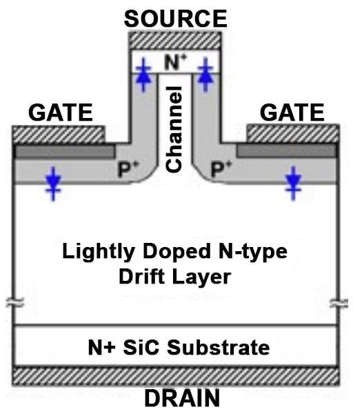
Figure 1: Cell structure of SiC trench JFET
In the on-state, if the gate-source voltage is 0V, the channel region is not depleted. A low resistance current path exists directly from the source to the drain. As the current increases, the potential at the drain side of the channel increases. When the potential difference between the drain and the gate reaches the 6V threshold, the channel pinches off and the current saturates.
Co-packaged SiC Cascode Structure
Figure 2a shows the structure of the co-packaged SiC cascode, where a customized low-voltage silicon MOSFET is connected in series with a SiC normally-on JFET to implement a normally-off device [2, 3]. The equivalent circuit of the cascode is shown in Figure 2b. Figure 3 shows the typical on-state characteristics of 1200V-60mΩ SiC co-packaged cascode. The cascode device has a threshold voltage (VTH) of 4.5V and is fully enhanced for the gate voltage (VGS) values above 10V.
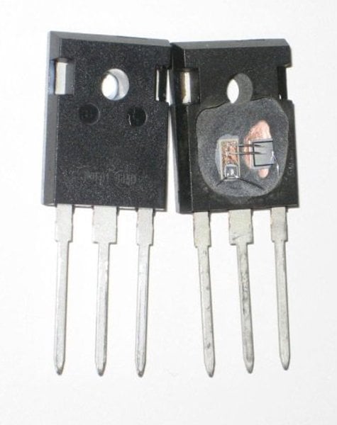
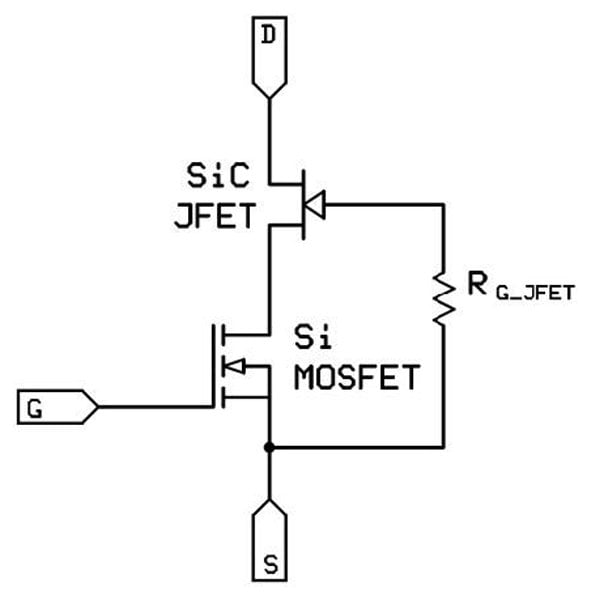
Figure 2: Co-packaged SiC cascode in TO-247 package (a) and equivalent circuit (b)
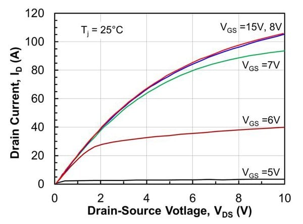
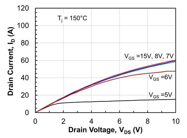
Figure 3: Typical on-state characteristics of 1200V-60mΩ co-packaged SiC cascode at a junction temperature of 25°C (a) and 150°C (b).
The cascode is switched on by turning on the low-voltage MOSFET. Since the MOSFET drain-source voltage drop (VDS) is small (ID*RDS(ON)), the JFET gate-source voltage (VGS) is near 0V in the on-state and the channel can conduct. When the low voltage MOSFET is turned off, the drain potential rises. The MOSFET VDS appears as a negative VGS on the SiC JFET, turning it off.
Inductive Switching Behavior
For the cascode devices, the turn-on tends to be significantly slower than the turn-off, so the commonly recommended gate drive circuit uses a low gate resistor for turn-on (RG_ON: 0-4.7Ω), and a large gate resistor for turn-off (RG_OFF: 10-50Ω) as shown in Figure 4. A ferrite bead can be used at the gate lead to reduce ringing. PCB layout techniques that help to minimize the gate-drain coupling due to stray capacitances are necessary because of the high dv/dt and di/dt that can occur in the SiC cascode during turn-off.
To aid with the discussion that follows, a term VGPJ referred as the plateau voltage is defined for the JFET:
VGPJ=VTHJ+ID/gmJ (1)
This term corresponds to the voltage seen in the gate-charge curve at a load current of ID. Here, gmJ is the JFET trans-conductance and VTHJ is the JFET threshold voltage.
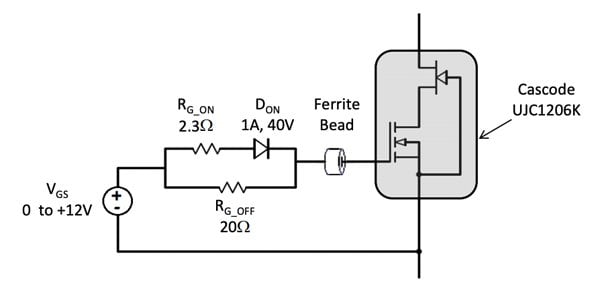
Figure 4: Recommended gate drive for SiC cascode
Turn-on: Figure 5a shows the typical turn-on waveforms of the SiC cascode. The turn-on process is initiated by raising the gate-source voltage (VGS_M) of the MOSFET, then the drain-source voltage (VDS_M) of the MOSFET falls and the gate-source voltage (VGS_J) of the JFET increases because the VDS_M is equal to -VGS_J. The VDS_M holds at a value close to -VGPJ, meaning that the VGS_J of the JFET is held at the plateau voltage VGPJ which is just sufficient for the JFET to handle the load current. The current ramps up in the JFET and the MOSFET simultaneously. The MOSFET VGS_M is still at its plateau voltage at this stage. Once the current reaches the load current (plus any extra current to recover the freewheeling diode), the MOSFET VDS_M falls towards ID*RDS(ON), and finally, the cascode VDS falls.
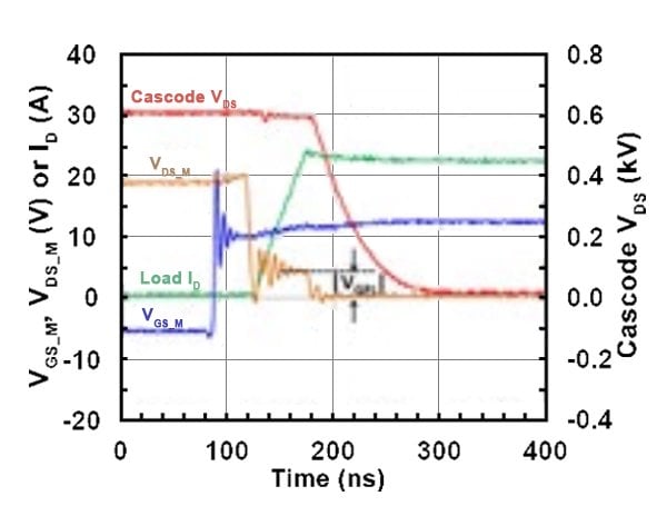
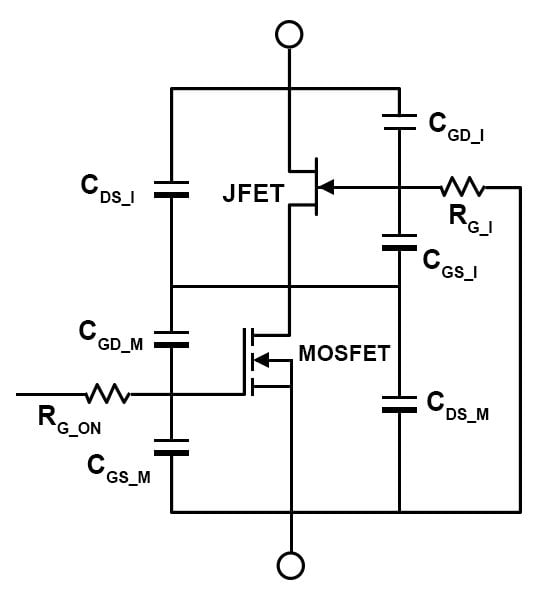
Figure 5: Measured turn-on waveforms of a 1200V SiC cascode under an inductive load condition (a) and equivalent circuit of the cascode (b)
The turn-on di/dt is limited by stray inductance at the MOSFET source and between the MOSFET drain and JFET source. It can be controlled well by the resistor (RG_ON) in series with the MOSFET gate. The turn-on dv/dt can be better understood using the equivalent circuit as depicted in Figure 5b, where the stray inductances are not included for clarity. If the RG_ON is small, the MOSFET turns on fast. The discharge rate of the drain-source voltage of the cascode is mainly determined by the discharge rate of the gate-drain capacitance (CGD_J) of the JFET because the JFET has near zero drain-source capacitance (CDS_J << CGD_J). The load current is flowing through the conducting channel of the JFET while the voltage falls. Displacement current through the internal gate resistor (RG_J) of the JFET discharges the CGD_J and drives the JFET gate to a more negative potential. Since the JFET gate cannot be driven too far negative without choking off the channel load current, the JFET VGS_J will stay at VGPJ. Therefore the maximum current through RG_J will set the maximum value of the turn-on dv/dt based on the following equation:
(VGPJ- ID*RDS(ON))/RG_J = CGD_J*dv/dt (2)
In this manner, the gate resistance RG_J of the JFET can be used to slow down the turn-on dv/dt. On the other hand, a lower RG_J and higher |VGPJ| value (more negative VTHJ for the JFET) can be used to obtain a faster turn-on.
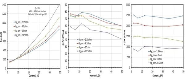
Figure 6: Measured turn-on energy loss (a), dv/dt rate (b) and di/dt rate of the 1200V-60mΩ SiC cascodes (UJC1206K) under a 600Vbus inductive load condition with the same device as a freewheeling diode.
Figure 6 shows the effects of the turn-on gate resistor RG_ON on the energy loss, dv/dt rate and di/dt rate of USCi’s SiC cascode (UJC1206K) during the turn-on transient. For low values of RG_ON, the dv/dt is controlled by equation (2). For large values of RG_ON, dv/ dt can be controlled by slowing the transition of the MOSFET drainsource voltage (VDS_M), which is equivalent to slowing down the gate turn-on voltage of the JFET.
Turn-off: Figure 7 shows the typical turn-off waveforms of the SiC cascode. The turn-off transient is initiated by turning off the MOSFET gate. After a delay (determined by RG_OFF*CISS_MOSFET), the drainsource voltage (VDS_M) of the MOSFET rises. The VDS_M is clamped to the avalanche breakdown voltage of the MOSFET and is seen to hold there during the period the drain-source voltage of the cascode rises. This generates a negative voltage between the gate and source of the JFET to turn off the JFET. Since the JFET still conducts the load current during the voltage rise, the gate-source voltage VGS_J of the JFET has to stay at the plateau voltage VGPJ in order to sustain that current. The drain-source capacitance CDS_J of the JFET is nearly zero, so there is very little current flowing through that path to the MOSFET gate, meaning that the cascode has very little Miller current. As the drain-source voltage of the cascode rises, its slope (dv/dt) is again dominated by the charging rate of CGD_J through the JFET internal gate resistor RG_J. The maximum current that can pass through RG_J is given by:
I G(RG_J) = {BV(MOSFET)-VGPJ} / RG_J = CGD_J*dv/dt (3)
Again, the maximum dv/dt can be limited by controlling RG_J. The turn-off dv/dt can also be reduced by using the MOSFET with a lower avalanche breakdown voltage and the JFET with a larger plateau voltage VGPJ (more negative threshold).
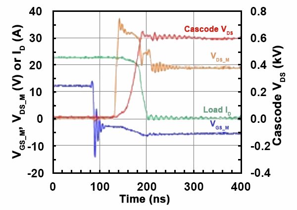
Figure 7: Measured turn-off waveforms of a 1200V SiC cascode under an inductive load condition
Once the drain-source voltage of the cascode reaches the bus voltage, the current rapidly decays as the JFET gate discharges. The discharge time constant depends on RG_J*CGS_J, and is also slowed down by the common source parasitic inductance in the gate loop of the JFET. The drain-source voltage of the MOSFET during the current fall in Figure 7 is set by its off-state value plus the voltage spike induced by the parasitic inductances between the drain and source terminals of the MOSFET. Once the current ramp is finished, the MOSFET VDS_M stabilizes quickly at a voltage needed to hold the JFET off.
Figures 8 shows the effects of the turn-off gate resistor RG_OFF on the energy loss, dv/dt rate and di/dt rate of USCi’s SiC cascode (UJC1206K) during turn-off transient. For low values of RG_OFF, the dv/dt is controlled by equation (3). For large values of RG_OFF, dv/dt and di/dt can be controlled by slowing down the transition of the MOSFET drain-source voltage VDS_M, which is equivalent to slowing down the turn-off gate voltage of the JFET. However, this comes at the cost of a longer delay time proportional to RG_OFF*Ciss_MOSFET.
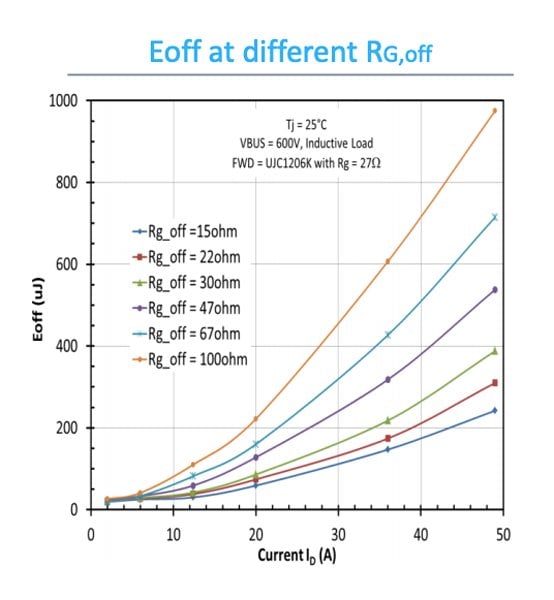
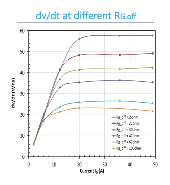
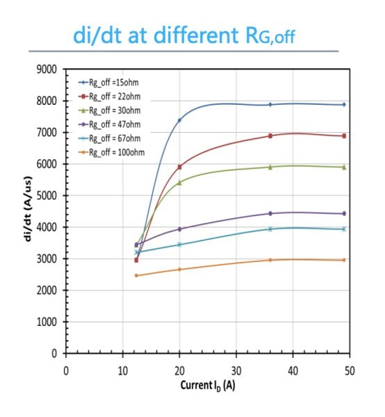
Figure 8: Measured turn-off energy loss (a), dv/dt rate (b) and di/dt rate of the 1200V-60mΩ SiC cascodes (UJC1206K) under a 600Vbus inductive load condition with the same device as a freewheeling diode
The low-voltage MOSFET used for USCi’s SiC cascodes is custom designed to have a built-in voltage clamp in order to make it operate safely in avalanche mode. Figure 9 shows the general concept of how this is accomplished by creating a low breakdown region between cells to carry the entire breakdown current. USCI Cascodes are 100% avalanche tested at final test.
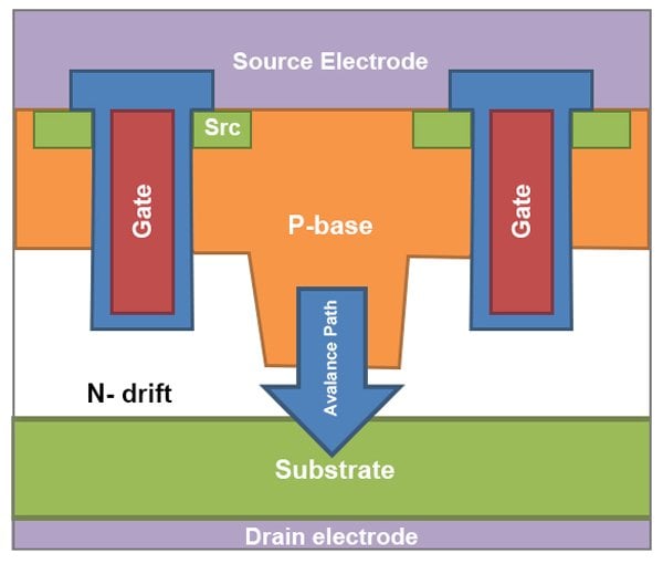
Figure 9: Low-voltage silicon MOSFET designed with an avalanche clamp to control cascode switching speed
During device development, stress tests are performed to ensure that all sampled devices pass 106 cycles of unclamped inductive switching (UIS). In addition, the MOSFET is qualified by the burn-in test when biased into avalanche for 1000hrs at a junction temperature of 150°C. As shown in Figure 10, negligible parameter shifts are observed after the burn-in test. The standalone MOSFETs are also tested to ensure that all sampled devices pass 106 cycles of UIS. With these precautions, the cascode can be used with the low-voltage MOSFET acting as the voltage clamp to limit its maximum turn-off speed.
ZVS Turn-on behavior: The ZVS turn-on behavior of the USCi cascode is also different from other cascode devices due to the fact that the trench JFET has almost zero drain-source capacitance CDS_J. Consider the situation where the cascode voltage is rapidly decreasing to zero while the MOSFET is still off. Since CDS_J is nearly zero, all the displacement current has to flow into the CGD_J path. There is no voltage balancing concern between CDS_J and the capacitances tied to the drain of the MOSFET (CGD_M + CDS_M + CGS_J) because the latter capacitance is much larger. This means that the accidental turn-on of the JFET due to high dv/dt [4, 5] can be avoided, making USCi’s SiC cascodes very well suited for applications with ZVS turnon and hard turn-off.
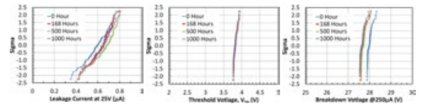
Figure 10: Measured shifts in the leakage current at 25V (a), threshold voltage (b), and breakdown voltage at 250µA (c) of the low-voltage silicon MOSFETs before and after 1000 hours of avalanche-mode burn-in at 150°C.
Summary
USCI’s co-packaged cascode device offers ease of use benefits to power system designers, requiring minimal modification of existing designs from the gate drive standpoint, and reducing cost by eliminating the need for an anti-parallel SiC diode. The high speed turn-off behavior requires attention to layout to mitigate EMI issues, so as to extract maximum benefit from the fast switching speed of the cascode structure. Given the avalanche and short-circuit ruggedness of the device, along with its excellent body diode, the device is well suited to a wide range of high performance circuits. Parts may be purchased directly on USCi’s website from May 1, 2015.
About the Authors
Anup Bhalla works as the Vice President of Engineering at United Silicon Carbide, Inc. where he is responsible for commercializing SiC-based Diodes, trench vertical JFETs, BJTs, trench vertical MOSFETs, GTOs and ICs. He earned his Bachelor's Degree in Electrical Engineering at the Indian Institute of Technology. He also holds a Master's Degree and Doctorate Degree in Electrical Engineering both earned at the Rensselaer Polytechnic University.
John Bendel works as the Senior Director for Business Marketing at United Silicon Carbide, Inc. since May 2014 where he is skilled in the field of semiconductors and power management. He earned his Bachelor's Degree in Electrical Engineering at the University of California, Davis.
Xueqing Li received the B.S. degree in electrical engineering from Tsinghua University, Beijing, China, in 1990, the M.S. degree in physical electronics and optoelectronics from the Institute of Electronics, Chinese Academy of Sciences, Beijing, in 1993, and the PhD degree in electrical and computer engineering from Rutgers University, Piscataway, NJ, in 2005. Since 2003, he has been a Senior Research Engineer with United Silicon Carbide, Inc., New Brunswick, NJ, where he is responsible for the design and simulation of power devices in 4H-SiC, creation of PSpice model of power semiconductor devices, and simulation of switching-mode power converter systems.
References
- Bhalla, Anup; Bendel, John; and Li, Xueqing, “Robustness of SiC JFETs and Cascodes,” Submitted to the Magazine of Bodo’s Power Systems.
- Li, Xueqing; Bhalla, Anup; Alexandrov, Petre; Hostetler, John; and Fursin, Leonid, “Investigation of SiC Stack and Discrete Cascodes,” Proceedings of PCIM Europe 2014, May 20-22, 2014, Nuremberg, Germany.
- Bendel, John and Li Xueqing, “Using “Normally on” JFETs in Power Systems,” Magazine of Bodo’s Power Systems, March 2015, pp.40-43.
- Huang, X.; Liu, Z.; Lee, Fred C; and Li, Q., “Characterization and Enhancement of High-Voltage Cascode GaN Devices,” IEEE Transactions on Electron Devices, Vol. 62, No. 2, February 2015, pp. 270-277.
- Bahl, S. R. and Seeman, M. D., “New Electrical Overstress and Energy Loss Mechanisms in GaN Cascodes,” Proceedings of APEC 2015, March 15 – 19, 2015, Charlotte NC, USA, pp.1262-1265.