Facebook
 Google
 GitHub
 Linkedin
State of the SiC MOSFET: Device evolution, technology merit, and commercial prospects
This article features Littelfuse Inc. SiC MOSFET device evolution, technology merit, and commercial success and substantial role for green energy movement.
Introduction
Insulated Gate Bipolar Transistor (IGBT) is a disruptive power transistor, first commercialized in the early 1980s, has had an enormous positive impact on the power electronics industry, enabling innovative converter design, improved system efficiencies, and worldwide energy savings. Indeed, some estimates suggest that the IGBT has helped forestall 75 trillion pounds of CO2 emissions over the past 25 years [1].
Today, the IGBT wide bandgap semiconductor silicon carbide (SiC) shows increasing promise for revolutionizing the power electronics world once again. The IGBT gave us a transistor simultaneously capable of blocking high voltages with low on-state (i.e., conduction) losses and well-controlled switching. The device is limited, however, in how fast it may be switched, which leads to high switching losses, large and expensive thermal management, and a ceiling on power conversion system efficiency. The beginning of SiC transistors eliminates an IGBT’s switching losses for similar ON-state losses (lower, actually, at light load) and voltage blocking capability, enabling unprecedented efficiency in addition to the reducing the over all weight and size of the system.
Like most disruptive technologies, however, the evolution of commercial SiC power devices has traveled a tumultuous road. This article is intended to put the evolution of the SiC MOSFET in context, and – along with an abridged history of the device’s advancements – present its technology merits today and its commercial prospects for the future.
History of Silicon Carbide or SiC
Since the 1970s, device-related SiC materials such as the MOSFET have been researched, but the use of SiC in power devices was formally suggested in 1989 [2]. Baliga’s figure of merit served as additional motivation for aspiring materials and device scientists to continue advancing SiC crystal growth and device processing techniques.
In the late 1980s, intense efforts were underway around the world to improve the quality of SiC substrates and hexagonal SiC epitaxy – needed for vertical SiC power devices – at places ranging from institutes like Kyoto University and AIST in Japan to the Ioffe Institute in Russia to the University of Erlangen and Linkoping in Europe to SUNY-Stony Brook, Carnegie Mellon, and Purdue University in the United States, to name just a few. The improvements continued throughout much of the 1990s until the first commercial device was released in 2001 in the form of a SiC Schottky diode by Infineon.
For a few years following their release, SiC Schottky diodes experienced field failures that were traced to material quality and device architecture. Rapid and drastic progress was made to improve the quality of substrates and epitaxy; meanwhile, a diode architecture known as the junction barrier Schottky (JBS) was used which more optimally distributed the peak electric field.
In 2006, the JBS diode morphed into what is now called the merged p-n Schottky (MPS) structure, which maintains optimal field distribution but also allows for enhanced surge capability by incorporating true minority carrier injection [3]. Today, SiC diodes are so reliable that they have demonstrated even more favorable FIT rates than silicon power diodes [4].
MOSFET Alternatives
The first SiC power transistor released to the market came in 2008 in the form of a 1200 V junction field effect transistor (JFET). SemiSouth Laboratories followed the JFET approach because, at the time, the bipolar junction transistor (BJT) and MOSFET alternatives had impediments that were thought to be insurmountable. Although the BJT had impressive current-per-active-area figures, the device had three major shortcomings:
First, the high current required to switch the BJT was frowned upon by many designers accustomed to using voltage-controlled devices like the MOSFET or IGBT.
Second, the BJT’s drive current is conducted across a base-emitter junction with a large built-in potential, leading to substantial power losses.
Third, because of the bipolar action of the BJT, it was particularly susceptible to a device-killing phenomenon known as bipolar degradation [5].
The JFET, on the other hand, is hindered by the fact that it is normally on the device, which can scare away many power electronics designers and safety engineers. Of course, it is possible to design around this, but simplicity and design elegance are underrated virtues in the engineering world. SemiSouth also had a normally-OFF JFET, but it proved far too difficult to manufacture in volume.
Today, USCi, Inc. offers a normally on SiC JFET co-packed with low-voltage silicon MOSFET in a cascode configuration [6], an elegant solution for many applications. Nevertheless, the holy grail of SiC power devices has always been the MOSFET due to its similarity in control to the silicon IGBT – but with the aforementioned superiority in performance and system benefits.
Evolution of the SiC MOSFET
The SiC MOSFET has had its share of issues, most of which are directly related to the gate oxide. The first signs of trouble were observed in 1978 when researchers at Colorado State University measured a messy transition region between the pure SiC and the grown SiO2 [7]. Such a transition region was known to have high densities of interface states and oxide traps that inhibit carrier mobility and lead to instabilities in threshold voltage; this would later be proven true by too many research publications to name.
Many in the SiC MOSFET research community spent the late 1980s and 1990s further studying the nature of various interface states in the SiC-SiO2 system.
Research in the late 1990s and early 2000s led to remarkable improvements in understanding the sources of interface states (whose density is abbreviated Dit), as well as reducing them and mitigating their negative effects. To mention a few noteworthy discoveries, oxidation in a wet environment – that is, using H2O as an oxidation agent instead of dry O2 – was observed to reduce Dit by two to three orders of magnitude [8].
Also, the use of off-axis substrates was found to reduce Dit by at least an order of magnitude [9]. Last, the effects of post-oxidation annealing in nitric oxide – a process commonly called nitridation – were first discovered by Li and co-workers in 1997 to reduce Dit to very low levels [10]. This was subsequently affirmed by six or seven other groups, a set of work that is nicely summarized in a paper by Pantelides [11]. It would be an egregious omission, of course, not to underscore the seminal contributions made by the bulk growth and wafer research community, who have taken us from mere Lely platelets to 150 mm wafers that are virtually free of device-killing micropipes.
Published research progress on the SiC MOSFET slowed somewhat over the next few years, as hopeful suppliers were busy making advancements they wanted to commercialize. However, the stage had been set for final improvements directed at further tightening threshold voltage stability as well as process enhancements and screening to ensure reliable gate oxides and completion of device qualification. In essence, the SiC community was getting ever closer to finding the holy grail.
Today’s MOSFET Quality
In just the past two years, commercially available 1200 V SiC MOSFETs have come a long way in terms of quality. Channel mobility has risen to suitable levels; oxide lifetimes have reached an acceptable level for most mainstream industrial designs, and threshold voltages have become increasingly stable.
What is equally important from a commercial standpoint is that these milestones have been reached by multiple suppliers, the importance of which is saved for a later section. Here, we substantiate claims of today’s SiC MOSFET quality, including long-term reliability, parametric stability, and device ruggedness.
Using accelerated time-dependent dielectric breakdown (TDDB) techniques, the oxide lifetime of Monolith Semiconductor’s MOS technology has been predicted by researchers at NIST to exceed 100 years, even at junction temperatures higher than 200 °C [12].
The NIST work used lifetime acceleration factors of applied electric field across the oxide (greater than 9 MV/cm) and junction temperature (up to 300 °C); for reference, oxide electric fields used in practice are around 4 MV/cm (corresponding to VGS = 20 V), and junction temperatures during operation are typically lower than 175 °C. It is also worth noting that while a temperature-dependent acceleration factor is commonly seen in silicon MOS, it had not been seen by NIST for SiC MOS prior to their work with devices from Monolith Semiconductor.
Next, threshold voltage stability has been convincingly demonstrated, as seen in Figure 1. High-temperature gate bias (HTGB) was performed at a junction temperature of 175 °C and under negative (VGS = -10 V) and positive (VGS = 25 V) gate voltages. As dictated by JEDEC standards, 77 devices from three different wafer lots were tested, and no significant shift has been observed.
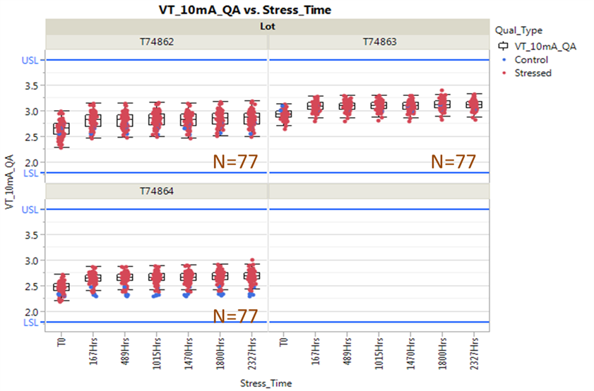
Figure 1: (a) Negative, VGS = -10 V and (b) positive, VGS = 25 V, high-temperature gate bias (HTGB) stress tests performed at 175 °C on 77 devices from three different wafer lots out to 2300 hours. The negligible deviation was observed.
Still another parameter set proven to be stable over the long term is the blocking voltage and OFF-state leakage of our MOSFETs. Figure 2 shows a high-temperature reverse bias (HTRB) test data.
More than eighty samples were stressed for 1000 h at VDS = 960 V and Tj = 175 C, after which post-stress measurements revealed no change in drain leakage or blocking voltage. With respect to device ruggedness, preliminary measurements shown in Figures 3 and 4 reveal short-circuit withstand time of at least 5 microseconds and an avalanche energy of 1 J.
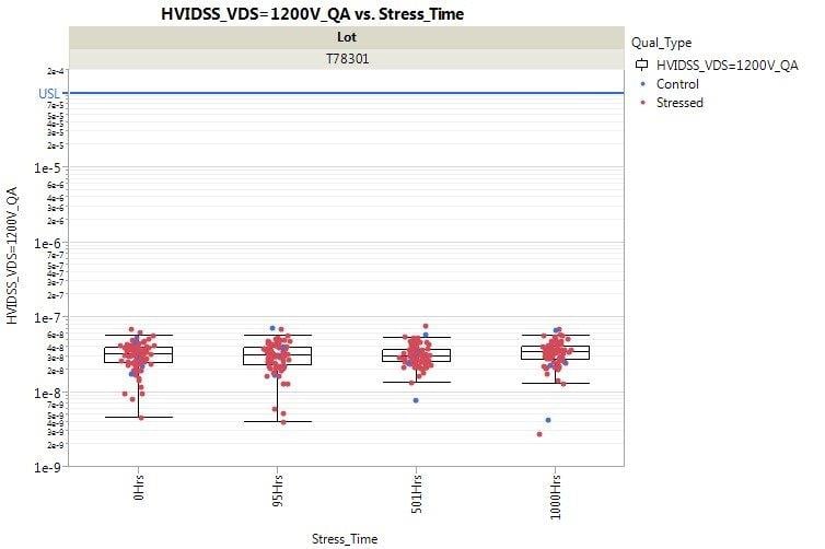
Figure 2: High-temperature reverse bias test data on 82 samples after 1000 h of stress at VDS = 960 V and Tj = 175 °C, illustrating no change in (a) drain leakage at VDS = 1200 V or (b) blocking voltage at ID = 250 μA.
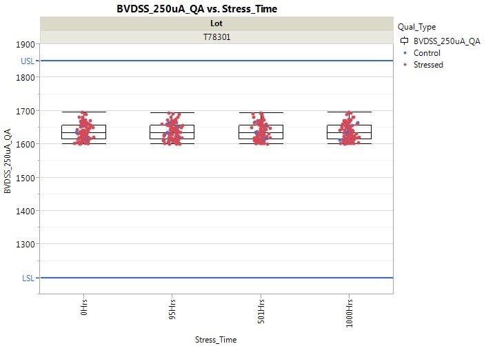
Figure 3: Short-circuit testing of a 1200 V, 80 mΩ SiC MOSFET at a dc link of 600 V and VGS = 20 V, indicating a withstand time of at least 5 μs.
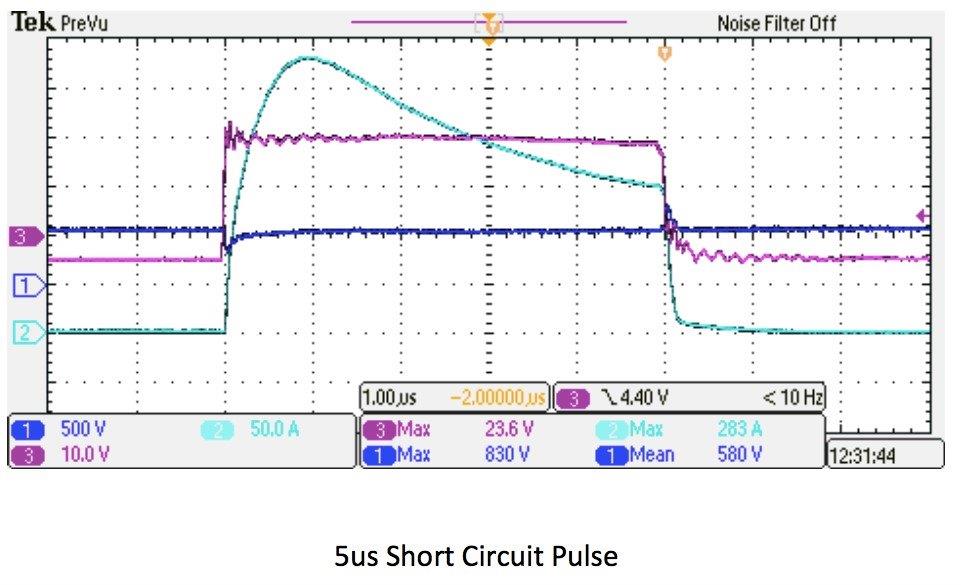
Figure 4: Avalanche ruggedness test on a 1200 V, 80 mΩ SiC MOSFET, showing that 1.4 J of energy was safely absorbed in the device with Ipeak = 12.6 A and L = 20 mH.
Although we cannot speak to the long-term reliability or ruggedness of other manufacturers’ products, we can say that based on our evaluation of commercially available SiC MOSFETs, there now appear to be multiple suppliers in the marketplace capable of supplying production-level quantities of SiC MOSFETs. These devices appear to have acceptable reliability and parametric stability, which will surely encourage mainstream commercial adoption.
Commercial Prospects
In addition to quality improvements, the past few years have seen tremendous commercial progress. Multiple SiC MOSFET suppliers are available to satisfy customers’ second-source concerns in addition to creating a competitive landscape that is good for both suppliers and users.
As previously mentioned, the fact that multiple SiC MOSFET suppliers have adequately reliable devices has been an enormous advancement, given the device’s lengthy evolution. Figure 5, reproduced with permission from Yole Développement’s “2016 Power SiC” report [13], shows the status of SiC MOSFET activities from various suppliers as of July 2016. Commercially available parts have been released from Wolfspeed, ROHM, ST Microelectronics, and Microsemi; the community can expect offerings soon from Littelfuse and Infineon.
![Status of SiC MOSFET development activities by various suppliers [13, reproduced with permission]](https://eepower.com/uploads/thumbnails/865-1312-littelfuse-monolith-semiconductor.jpg)
Figure 5: Status of SiC MOSFET development activities by various suppliers [13, reproduced with permission].
Multi-chip power modules are also a hot topic in the SiC world among customers and suppliers alike. Figure 6, also taken from Yole’s Développement’s 2016 report [13], shows the status of SiC module development activities. We believe many bright opportunities remain for SiC MOSFETs in discrete packages, as best layout practices of both the control and power circuits can easily extend the applicability of discrete solutions to tens of kilowatts. Higher power levels and the motivation to simplify system design will drive SiC module development efforts, but the importance of optimizing parasitic inductance from the package, control circuit, and surrounding power components cannot be overstated.
![Status of SiC power module development activities [13, reproduced with permission]. Blue circles represent modules with only SiC devices, while orange circles depict modules that use silicon transistors and SiC diodes](https://eepower.com/uploads/thumbnails/865-1313-littelfuse-monolith-semiconductor.jpg)
Figure 6: Status of SiC power module development activities [13, reproduced with permission]. Blue circles represent modules with only SiC devices, while orange circles depict modules that use silicon transistors and SiC diodes.
The final elephant in the room when it comes to the commercial prospects of the SiC MOSFET is a price. Our view on price erosion is favorable, largely due to two aspects of our approach: first, our devices are manufactured in an automotive-grade silicon CMOS fab; second, the process is run on 150 mm wafers.
This is explained in greater detail in a separate work [14], but suffice it to say that the central advantages of utilizing existing silicon CMOS fabs are the absence of capital expenses and an optimization of operating expenses, both of which would otherwise be passed to the end customer.
Furthermore, manufacturing on 150 mm wafers produces more than double the devices as compared to 100 mm wafers, which dramatically impacts the per-die cost. Some indication of pricing is given in Figure 7, based on a survey taken from commercially available SiC MOSFETs at Digi-Key.
As an example, since the first announcement at Digi-Key six years ago, the price of a 1200 V, 80 mΩ device in TO-247 has fallen by more than eighty percent, even if the SiC MOSFET is still 2-3x more expensive than a comparable silicon IGBT.
Designers are already viewing substantial system-level price benefits using SiC MOSFETs over Si IGBTs at today’s price levels, and we expect SiC MOSFET pricing will continue to fall as an economy of scale takes hold with 150 mm wafers.
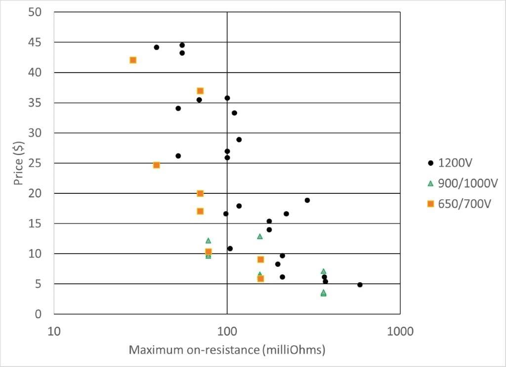
Figure 7: Price survey of commercially available SiC MOSFETs as seen at Digi-Key.
Conclusions
The silicon IGBT was an enormous positive disruption to the power electronics community in the 1980s, and it has been the workhorse of the industry ever since. The next revolutionary technology will be the SiC MOSFET.
Today’s state of the SiC MOSFET indicates resolution on major commercial impediments including price, reliability, ruggedness, and diversification of suppliers. In spite of a price premium over Si IGBTs, the SiC MOSFET has already seen success due to cost-offsetting system-level benefits; the market share for this technology will increase sharply over the next few years as materials costs fall. After more than forty years of development effort, at last, the SiC MOSFET appears poised for widespread commercial success and a substantial role in the green energy movement.
About the Authors
Dr. Kevin M. Speer achieved his PhD in Electrical Engineering at Case Western Reserve University. He has experienced in the development of product strategy and technology roadmap in alignment with market needs, available resources, and accessible technical competency. Skilled in the establishment of technical & business relationships with international market leaders and government funding agencies. He become a global manager for technology strategy and business development at Littelfuse, which the company products are vital components in applications that use electrical energy, from consumer electronics to vehicles and industrial facilities.
Dr. Sujit Banerjee accomplished his PhD in Electrical Engineering at Rensselaer Polytechnic Institute. He has 15 years of experience in silicon and SiC high-voltage technology, in which he is a CEO at Monolith Semiconductor which is a company that is acquired by Littelfuse Incorporated. Then, he become a director for SiC products at Littelfuse, in which the company products are vital components in applications that use electrical energy, from consumer electronics to vehicles and industrial facilities.
Reference
- B. J. Baliga, “Social impact of power semiconductor devices.” Proc. of IEEE International Electron Devices Meeting, 2014.
- B. J. Baliga, “Power semiconductor device figure of merit for high frequency applications.” IEEE Electron Device Letters 10 (10), 1989.
- R. Rupp, M. Treu, S. Voss, F. Bjork, and T. Reimann, “2nd Generation SiC Schottky diodes: A new benchmark in SiC device ruggedness.” Proc. of IEEE International Symposium on Power Semiconductor Devices and ICs, 2006.
- T. Barbieri, “Technical Article: SiC Schottky Diode Device Design: Characterizing Performance & Reliability.” Wolfspeed
- M. Treu, R. Rupp, and G. Sölkner, “Reliability of SiC power devices and its influence on their commercialization – review, status, and remaining issues.” Proc. of IEEE International Reliability Physics Syposium, 2010.
- United SiC Cascodes.
- R. W. Kee, K. M. Geib, C. W. Wilmsen, and D. K. Ferry, “Interface characteristics of thermal SiO2 on SiC.” Journal of Vacuum Science and Technology 15 (4), 1978.
- S. M. Tang, W. B. Berry, R. Kwor, M. V. Zeller, and L. G. Matus, “High frequency capacitance-voltage characteristics of thermally grown SiO2 films on β-SiC.” Journal of the Electrochemical Society 137 (1), 1990.
- H. Yano, T. Kimoto, and H. Matsunami, “Interface States of SiO2/SiC on (11-20) and (0001) Si Faces.” Materials Science Forum, vols. 353-356, 2001.
- H. Li, S. Dimitrijev, H. B. Harrison, and D. Sweatman, “Interfacial characteristics of N2O and NO nitride SiO2 grown on SiC by rapid thermal processing.” Applied Physics Letters 70 (15), 1997.
- S. Pantelides et al., “Si/SiO2 and SiC/SiO2 Interfaces for MOSFETs – Challenges and Advances.” Materials Science Forum, vols. 527-529, 2006.
- Z. Chbili, K. P. Cheung, J. P. Campbell, J. Chbili, M. Lahbabi, D. Ioannou, and K. Matocha, “Time Dependent Dielectric Breakdown in high quality SiC MOS capacitors.” Materials Science Forum, vol. 858, 2015.
- Yole Développement, “Power SiC 2016: Materials, Devices, and Applications.” July 2016.
- S. Banerjee, K. Matocha, K. Chatty, J. Nowak, B. Powell, D. Gutierrez, and C. Hundley, “Manufacturable and Rugged 1.2 kV SiC MOSFETs Fabricated in High-Volume 150 mm CMOS Fab.” To be presented in Proc. of IEEE International Symposium on Power Semiconductor
This article originally appeared in the Bodo’s Power Systems magazine.