Facebook
 Google
 GitHub
 Linkedin
Rapid Power Prototyping Speeds up the Development of Custom High Performance Power Converters
This article discusses the reduction of risk in new system development of rapid prototyping of custom power electronics systems using modular technology.
Development of high-performance power electronic systems is a complex task involving the careful design of many different interdependent subsystems such as power stage, gate drivers, fault protection, digital circuits and embedded software.
Introduction
Most companies are resource-limited and under increasingly tight product development timescales. In order to lower the barrier to development and adoption of novel power electronic systems, Converter Technology has developed a rapid power prototyping technology platform to significantly reduce the time needed in the early stage of a project to get to first functional prototype.
Modular Concept
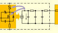
The modular concept shown in Figure 1 allows the first prototype of a new converter to be realised by using custom high-performance power electronic modules. System partitioning of the modules has been chosen carefully to separate the key functionality onto individual PCBs with a common interface. The mechanical arrangement allows a fully functional system ‘stack’ to be built which includes high-performance digital control, advanced gate drive/protection and power devices. This approach can prove out system performance at a very early stage in the project. Availability of early-stage prototype hardware is critical to de-risking overall project plans.

Figure 1: Modular Concept
A number of key features have been implemented into the platform from the outset:
- Highly modular architecture to allow for rapid system configuration
- SIC MOSFET based power boards currently support up to 15kW in a single system. Systems can be paralleled to provide higher power levels. Powerboards with other device types are currently under development.
- Custom advanced digitally addressable intelligent gate drive board suitable for driving many device types including MOSFETS, IGBT’s and new wideband gap transistors.
- DC link capability to 800V
- Control board based around high-performance 32-bit Delfino processors. The function and behaviour of the stack is defined in software and allows reconfiguration as the core part of most common isolated and non-isolated topologies including bidirectional two or four quadrant converters. Examples include three-phase AFE/inverter, multiphase buck or boost, resonant converters such as phase-shifted full bridge or LLC and hard-switched converters such as full bridge.
- The control board includes three 12-bit DACs which allow digital values within the control system to be output for display on a scope in real-time to aid system debug and analysis.
- Robust isolated CANBUS communications to ease integration into Labview automated test environment.
- Extensive fault monitoring and protection to allow the power stage to independently look after its own environment if key operating stress levels are exceeded. This protection prevents bugs in software during application development from damaging the power stage.
In addition to early-stage prototyping, the platform acts as a useful tool to aid in-depth learning about how different power topologies operate in practice. Since the behaviour is software-defined, the impact of switching frequency, duty cycle and phase relationship can be easily explored in real-time on real hardware. Closed-loop current or voltage control can be implemented along with custom soft-start algorithms.
Example Application – HV Synchronous Buck Converter
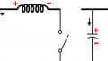
As an example of the flexible capability of modular technology, a stack was configured to explore the complex factors impacting conversion efficiency in a high voltage synchronous buck converter. The present stack system power board supports three Cree SIC MOSFET half-bridge legs so, for this set of tests, two of the switching legs were disabled and one leg configured to operate as a synchronous buck converter. An external power inductor and capacitor were used to complete the Synchronous buck power stage as shown in Figure 2.

Figure 2: Synchronous buck with external inductor and capacitor
In this example, the synchronous buck converter is operated under hard-switching conditions and of particular interest was the behaviour of the power conversion efficiency as a function of both load current and switching frequency. The CANBUS port was used to allow a custom Labview script to vary the power stage switching frequency as part of an automated test.
For the test, the input supply rail was set to 400V, the demand output set to 300V and efficiency was measured from input to output as a function of load current from 0 to 10A and switching frequency from 20kHz to 180kHz. The ability to automate the data capture allows many data points to be captured in a short timeframe. In the example here, 4000 individual efficiency measurements were taken over the range of load current and switching frequency in a two-hour period. Figure 3 shows the behaviour of the efficiency as a function of the two key variables whilst Figure 4 shows an equivalent contour plot highlighting regions of constant efficiency.

Figure 3: Efficiency as a function of two variables

Figure 4: Regions of constant efficiency
The actual shape of the surface plot shows an interesting region at lighter load currents where the efficiency peaks and then falls away. Consideration of the operating waveforms indicates that the region corresponds to the point whereby the forced synchronous operation results in a negative inductor current for part of the operating waveform. With bipolar inductor current, each switching transition becomes lossless due to natural commutation of the node voltage during the dead-time. This provides a temporary boost to the efficiency before the reduction in load current dominates the efficiency profile and efficiency falls again. The boundary conduction mode point is a function of switching frequency and load current as shown in equation 1.
`"IOUT"=(V_("in")*δ*(1-δ))/(2*"Fs"*L)`
Where Vin = Input Voltage (V), δ = duty cycle (p.u.), Fs = Switching Frequency (Hz) and L = Output Inductance (H)
For this particular example, the island of the highest efficiency of 99% occurs towards the maximum load current and at the lower end of the operating frequency range. Performance over the wider range of operating conditions is excellent. Figure 5 shows the clean operating waveforms possible with SiC devices with the switching node voltage shown on Channel 1 (Yellow) and inductor current on Channel 2 (Red).

Figure 5: Clean operating waveforms possible with SiC
Overall efficiency of the converter is impacted by all power loss mechanisms and these mechanisms are functions of the particular operating point of the converter. For example, wide bandgap devices such as SIC or GaN have low body capacitance and natively high-performance body diodes with negligible reverse recovery charge. This makes these parts suitable for high-frequency operation since reverse recovery and capacitive losses are minimal. IGBT’s and traditional MOSFETS would most likely show a stronger system level degradation in efficiency at higher frequencies which would change the location of the island of efficiency to a different point in the solution space.
IGBT switching loss is very much higher than MOSFETs and wide bandgap power devices so will tend to have an island of maximum efficiency at much lower frequency. However, at high load currents, the conduction loss of an IGBT can be much lower than that due to the Rdson of a MOSFET. For high current applications, IGBT based converters would show an efficiency plot which may exceed that of other technologies but only if the frequency was low and the demand current high enough to allow the conduction behaviour of the IGBT to dominate the loss mechanisms.
The loss mechanisms in the passives will be dominated by the inductor loss. Core loss and winding loss are strongly dependant on switching frequency and the ratio of DC to AC currents flowing. In general, a given inductor loss profile will reduce as the frequency comes down. However, at a certain point, the increased flux density variation will begin to dominate and the losses will begin to rise. The point of transition will be dependent on many aspects of the inductor design and their impact on overall efficiency will depend on how much other external loss mechanisms change with frequency.
Conclusions
Rapid prototyping of custom power electronics systems using modular technology can significantly reduce risk in new system development. Furthermore, the flexibility of software-defined function within the modular system allows the system to be re-tasked easily and can form the heart of a useful learning and experimentation platform. Converter Technology has used this approach now with multiple applications including high power LLC systems. Further applications under development using the platform include an Active Front End and multi-phase converters.
The system has proved robust and significantly enhances the productivity of the hardware teams using it.
About the Author
Dr. Iain Mosely works as the Technical Director of Converter Technology. He is responsible for ensuring that Converter Technology is always positioned to provide the highest quality custom power solutions to their growing global customer base. He is highly skilled in the field of power electronics, power supplies and electronics. He earned his PhD in Power Electronics at the University of Sheffield located in England.