Facebook
 Google
 GitHub
 Linkedin
Rohm Unleashes Gate Driver for Next-Gen GaN Power Designs
Rohm’s high-speed isolated gate driver IC is optimized for HV-GaN HEMTs.
From faster motor drives to higher-density power supplies, GaN semiconductors are rewriting the rules of power electronics. But unlocking their full performance takes more than just a new transistor; it requires equally advanced gate drive control. That’s where Rohm’s newest gate driver enters the equation.
Rohm’s BM6GD11BFJ-LB is a purpose-built isolated gate driver IC tailored specifically for high-voltage GaN HEMTs. Designed for switching frequencies up to 2 MHz and with support for minimum input pulse widths down to 65 ns, this compact driver unlocks the speed and efficiency GaN was meant to deliver while improving safety, signal integrity, and design simplicity in high-performance applications.

Rohm’s BM6GD11BFJ-LB gate driver delivers the speed, safety, and isolation. Image used courtesy of Rohm
Optimized Switching for GaN Power Applications
Unlike silicon or SiC transistors, GaN HEMTs demand extremely fast and precise gate drive characteristics to achieve their full efficiency potential. Rohm’s BM6GD11BFJ-LB is engineered from the ground up to meet this challenge, delivering clean and reliable switching at speeds up to 2 MHz. Its galvanic isolation barrier supports up to 2500 Vrms, ensuring safe signal transmission between control and power domains even in high-voltage designs.
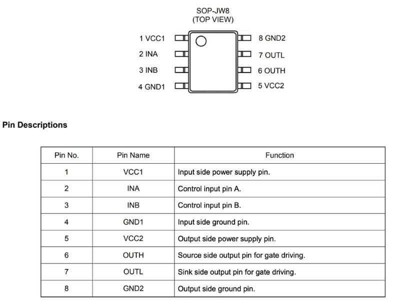
BM6GD11BFJ-LB pin configuration and description. Image used courtesy of Rohm
The device supports gate voltages between 4.5 V and 6.0 V, ideal for fully enhancing most GaN devices. Key enhancements include a maximum input-to-output delay of just 60 ns and a minimum input pulse width of 65 ns, 33% shorter than Rohm’s previous generation, making it suitable for aggressive duty cycle switching without losing control fidelity. Combined with the ability to operate across a wide temperature range from -40°C to +125°C, it’s well suited to harsh industrial and commercial environments.
On-Chip Isolation and CMTI Improvements
Rohm’s BM6GD11BFJ-LB gate driver uses a proprietary on-chip isolation design that helps cut down on parasitic capacitance, making it easier to switch at higher speeds with less EMI. By lowering that capacitance, the driver improves signal clarity and reduces the energy wasted during switching—key benefits when operating at high frequencies.
It also raises the Common Mode Transient Immunity to 150 V/ns, making it 50% higher than typical alternatives, delivering better noise rejection in high-slew environments common to GaN-based topologies like LLC resonant converters or bridgeless PFC stages. This is especially important for engineers designing in compact, high-voltage systems where tight PCB layouts can exacerbate coupling and noise issues.
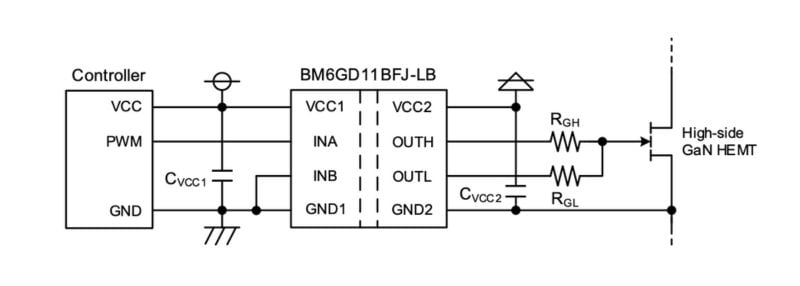
Basic circuit diagram. Image used courtesy of Rohm
Designers can independently tune the slew rate on rising and falling edges by adjusting resistors on separate source and sink driver pins. This provides fine control over EMI and switching losses, without requiring changes to the power stage or external gate driver circuitry. This tunability is particularly useful in applications where switching behavior must be balanced between noise emissions, thermal management, and switching speed.
Built-In Safety and Compact Packaging
The driver includes under-voltage lockout on both the input and output sides to ensure it only runs when supply voltages are within a safe range. This helps protect the gate driver and the GaN transistor from unstable conditions like voltage dips or transients that could cause misfiring or damage.
Combined with its compact SOP-JW8 package (4.9 × 6.0 × 1.65 mm), the BM6GD11BFJ-LB is a strong fit for high-density applications like server power supplies, AC adapters, motor drives, and GaN-based inverter systems. It is also a valuable choice for engineers targeting high-frequency wireless charging, telecom, and aerospace platforms where efficiency and weight are critical.
Low standby power (0.5 mA max on the output side) further reduces parasitic losses, making the device well-suited for eco-conscious designs, including those targeting compliance with upcoming international standby power regulations.
As wide bandgap power electronics continue to reshape high-efficiency design, Rohm’s BM6GD11BFJ-LB stands out as a gate driver built for the future of GaN. Its fast, isolated switching, compact footprint, and robust noise immunity offer engineers the tools to create more compact, efficient, and responsive power systems.