Facebook
 Google
 GitHub
 Linkedin
Infineon Intros 75 mΩ 650 V MOSFETs for Industrial Use
The CoolSiC G2 MOSFET variants expand cooling options and compact form factors to medium-power SMPS designs.
Infineon has introduced 75 mΩ variants to its CoolSiC MOSFET 650 V G2 portfolio, aiming at compact, high-density power systems. With growing system complexity and space constraints in industrial and consumer sectors, designers increasingly require thermally optimized and flexible power components. Infineon developed the 75 mΩ G2 MOSFETs to extend the CoolSiC platform’s applicability to systems where thermal cycling, EMI, and versatility are top priorities.
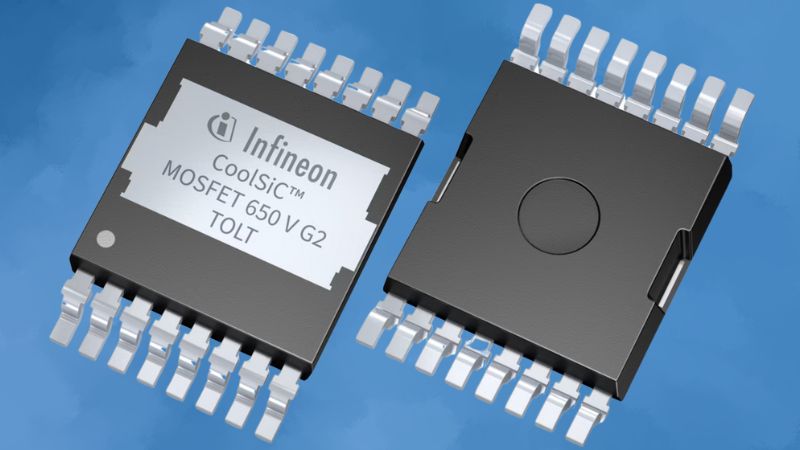
The CoolSiC MOSFET 650 V G2 options. Image used courtesy of Infineon
Second-Generation CoolSiC MOSFETs
The CoolSiC MOSFETs are based on Infineon’s second-generation (G2) silicon carbide trench architecture, with improved switching behavior, gate oxide reliability, and figures of merit relative to the previous generation. According to Infineon, these enhancements collectively allow for better efficiency and increased thermal and electrical robustness in high-power density environments.
The devices are available in discrete packaging options, including TOLL, ThinTOLL 8x8, TOLT, D2PAK, TO247-3, and TO247-4, and support both top-side cooling (TSC) and bottom-side cooling (BSC) architectures. Notably, all variants maintain avalanche capability and include an enlarged driving voltage window from -7 V to +23 V static for improved immunity against unwanted turn-on events relative to previous generations.
Infineon also notes that multiple package options lead to broader design flexibility within the series. For example, the TOLL and ThinTOLL 8x8 packages are optimized for high thermal cycle stability and efficient PCB layout, while the compact ThinTOLL 8x8 in particular extends package applicability to new design categories.
The TOLT package supports top-side cooling, offering up to 95% direct heat dissipation through the top interface. This performance allows designers to use both sides of the PCB for thermal routing, improving space utilization and minimizing parasitic inductances. Ultimately, by supporting both TSC and BSC approaches, the G2 MOSFETs accommodate varying thermal management requirements without compromising form factor constraints.
Top Side Cooling for Power Semiconductors
Top-side cooling is an advanced thermal management technique that allows heat dissipation through the top surface of a semiconductor package, in contrast to traditional bottom-side cooling, which relies on thermal contact with the PCB. TSC designs mount a heatsink or thermal interface material directly onto the component’s top for more efficient heat transfer to the ambient.
The primary advantage of TSC is spatial efficiency. By offloading heat through the top, PCB designers can reclaim the bottom side for routing or additional components in high-density or double-sided board layouts.
Thermal performance also improves. According to Infineon, TSC allows up to 95% of generated heat to be directly transferred away from the device, significantly reducing junction temperatures and enhancing reliability. Lower thermal resistance also allows for higher current handling without excessive derating.
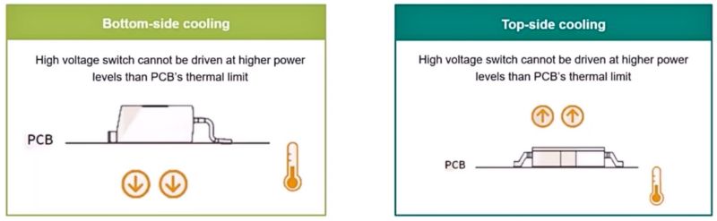
Bottom-side cooling and top-side cooling. Image used courtesy of Infineon
TSC is especially effective in environments where airflow is limited or when forced-air cooling must be minimized to reduce noise or cost. It also reduces thermal stress on solder joints and PCB materials by distributing thermal load more evenly, improving product lifecycle and resilience under thermal cycling.
However, designing with TSC does require mechanical adjustments, including clamping mechanisms and suitable heat spreaders. Still, the gains in thermal efficiency and PCB flexibility make it a compelling option in power-dense applications.
Modular Packaging Supports Scalable Design
Infineon’s CoolSiC 650 V G2 portfolio with 75 mΩ variants may provide system designers with tools to optimize their SMPS architectures' thermal, electrical, and mechanical aspects.