Facebook
 Google
 GitHub
 Linkedin
Argonne Researchers Jet-Print Durable, Low-Power Transistors
Argonne National Laboratory researchers have jet-printed durable transistors for flexible electronics.
Argonne National Laboratory and University of Chicago researchers have demonstrated aerosol‑jet‑printed transistors that switch at sub‑1‑V bias and survive thousands of cycles without degradation.
The devices rely on multicomponent nanoparticle inks and a redox‑gating scheme to modulate conductivity in vanadium dioxide (VO2), a correlated oxide with phase‑change behavior. The work targets flexible sensors, smart windows, and other low‑power systems where printed electronics have struggled with reliability and energy efficiency.

The aerosol-jet printer. Image used courtesy of Argonne National Laboratory
Printed Electronics Face Voltage and Reliability Limits
Printed electronics promise rapid, additive fabrication on plastics and other unconventional substrates, but mainstream methods often require high‑temperature sintering to achieve conductivity and adhesion. These conditions are incompatible with many polymers and with 3D or conformal surfaces.
Even when metallization is feasible at low thermal budgets, high operating voltages, short lifetimes, or drift associated with aggressive ionic/electrochemical gating have limited transistor‑level functions. Industry and research communities seek processes that combine low‑temperature, conformal patterning with device physics that enable low‑voltage, durable switching.
Aerosol Jet Printing Enables Low-Temperature Device Fabrication
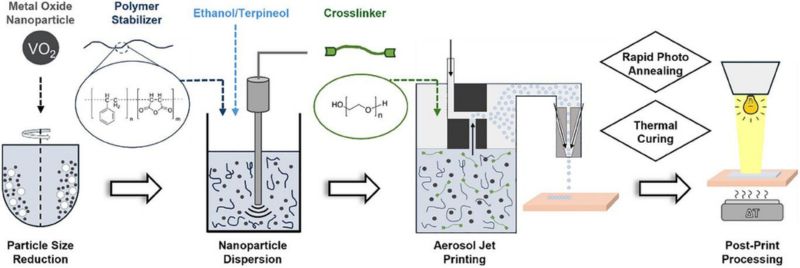
The Argonne team used aerosol jet printing (AJP), a maskless direct‑write method that atomizes functional inks into an aerosol and focuses them with a sheath gas to deposit fine features onto flat or 3D surfaces.
Because deposition and curing can be performed at comparatively low temperatures, AJP supports rapid prototyping on flexible substrates while building multilayer device stacks. In this case, custom inks containing vanadium dioxide (VO2) nanoparticles and complementary redox components are printed to form the transistor channel and gating architecture.
The transistor operates via redox gating rather than purely electrostatic field effect. A small, applied bias drives a controlled redox reaction at or near the VO2 surface, modulating carrier density and, in turn, the electronic phase and conductivity of the channel.
Unlike more aggressive ionic‑liquid gating that can induce irreversible defect formation, the reported solid‑state redox approach targets low‑voltage operation and material integrity. This offers a route to phase and resistance control in correlated oxides with modest energy input, potentially improving endurance.
Channel ink formulation and processing. Image used courtesy of Erwin et al.
To correlate ink formulation, print morphology, and device behavior, the researchers leveraged Argonne’s Center for Nanoscale Materials for nanoscale materials studies and the Advanced Photon Source for microprobe mapping and spectroscopy. The team conducted complementary high‑resolution X-ray work at Brookhaven’s National Synchrotron Light Source II. These platforms enable structural and elemental mapping that links nanoparticle assembly and film microstructure to electronic performance.
Sub-Volt Switching and Multi-Kilocycle Endurance
Key reported device metrics include switching at approximately 0.4–0.5 V, endurance exceeding 6,000 on/off cycles, and state transitions on ~1‑s timescales. These figures significantly raise the bar for printed, redox‑operated oxide devices.
The team also observed robust channel current modulation with small gate stimuli, illustrating low‑energy control of conduction in the printed VO2. These results indicate that redox gating can deliver stable, low‑voltage operation in a fully printed platform.
A notable aspect is durability. Prior printed devices using electrochemical control have often failed within tens of cycles due to irreversible chemistry or mechanical instability at interfaces. By contrast, the solid‑state redox system preserved channel functionality through thousands of cycles, suggesting that careful ink design and mild gating chemistry can mitigate degradation pathways. Structural and compositional mapping at APS and NSLS‑II further supported the stability narrative by tying device behavior to the as‑printed microstructure.
The researchers acknowledge that printed transistors fabricated here are larger and slower than CMOS counterparts, but emphasize that the aim is different. They focused on low‑power switching on unconventional form factors using accessible, additive manufacturing.
The paper in Advanced Materials points toward logic elements and neuromorphic concepts as the next targets, with machine‑learning‑assisted process optimization to navigate the many degrees of freedom in ink rheology, print parameters, and post‑processing.
Industry Implications
For electrical and power electronics engineers evaluating edge devices, building systems, or grid‑adjacent sensing, the ability to print low‑voltage, durable switches could simplify distributed instrumentation. Sub‑1‑V operation is compatible with energy‑harvesting nodes and thin‑film batteries, while solid‑state redox gating offers a path to a longer service life than ionic‑liquid approaches.
AJP’s conformal deposition also opens design space for embedding electronics onto curved housings, structural members, or laminated glazing—relevant to smart windows where VO2’s thermochromic behavior and electrically steered phase could enable adaptive optical and thermal control.
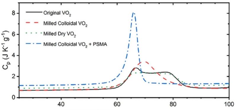
Specific heat capacity of VO2 ink films. Image used courtesy of Erwin et al.
Manufacturing flexibility is another advantage. AJP supports fine features and multilayer stacks at low temperatures, reducing tooling and enabling rapid iteration from design to test vehicles. Combined with DOE user‑facility characterization to shorten feedback cycles, this workflow could accelerate technology readiness for niche logic, memory‑like selectors, or analog switching elements that complement rather than compete with scaled CMOS.
Toward Practical Printed Hybrid Electronics
The work demonstrates a credible route to printed hybrid electronics that are both energy‑efficient and enduring—two attributes that have historically been difficult to achieve simultaneously in additively manufactured transistors.
By coupling multicomponent inks, aerosol jet deposition, and redox gating of VO2, the team achieved low‑voltage switching (~0.4–0.5 V) and multi‑kilocycle endurance, supported by advanced characterization at national user facilities.
Near‑term research directions include device miniaturization, faster response, and integration into logic or neuromorphic primitives, with machine learning proposed to optimize the complex print/materials parameter space. If these targets are met, engineers could gain a practical toolbox for conformal, low‑power electronics in applications ranging from structural health monitoring to adaptive building envelopes.