Facebook
 Google
 GitHub
 Linkedin
x-GaN 2.0: The Destination FiT10 is Demonstrably Exceeded
This article highlights Panasonic X-GaNTM transistors that is called as HD-GiT that aimed for power converters application in the ~100 W to ~5-6 kW range.
For more than 35 years, power MOSFETs have dominated the field of power converter design in the low to medium power range. This has been supported by continuous innovation in the components structure and related semiconductor technology. Fast switching characteristics and low losses, as well as ease of use in various circuit topologies also contributed to their success. At the dawn of a new millennium, however, silicon power MOSFETs are reaching their theoretical performance limits, which means that further progress in power supplies and power management systems will no longer be as easy to achieve with these switching elements.
Current trends in power supply unit design are focusing on higher efficiencies and power densities, that go beyond the capabilities of the silicon MOSFET technology. Development engineers need new switching devices that are able to meet these requirements. And so begins the conception of gallium nitride transistors (GaN).
Overview and Advantages of HD-GITs
Panasonic Hybrid Drain-Gate Injection Transistors (HD-GITs) are normally-off GaN-on-silicon transistors (Figure 1).

Figure 1. Normally off
They are based on the HEMT principle, using the highly mobile 2D electron gas forming at an AlGaN-GaN heterojunction as conduction layer. The active part of the transistor is completed on the top side with (ohmic) drain & source contacts, a recessed p-GaN gate (ohmic contact) and a p-GaN “gate like” structure connected to the drain. For cost reasons, the transistor is grown on top of 6 inches silicon wafers by MOCVD process. In order to reduce the tensile stress caused by the mismatched crystal lattices of Si and GaN, to limit the vertical drain-substrate leakage currents and to prevent deep breakdown paths in the conductive Si substrate, a lattice buffer layer (Figure 2) is inserted between the silicon bulk and the active top side of the transistor.

Figure 2. Lattice buffer
This buffer plays a central role in the determination of key reliability characteristics of the transistors as will be developed further below. The transistor is turned on resp. off like a field effect transistor, by applying a gate-source voltage above resp. below a threshold voltage. In off state, the p-GaN gate depletes the electron gas underneath by lifting the potential of the AlGaN-GaN junction. In on-state, the gate behaves essentially like a diode. Unlike in MOS transistors, a small (around 10mA) current is injected from the gate into the conducting layers by electrons tunneling through the AlGaN barrier. Due to the low velocity of holes in the GaN material, the current conduction at the AlGaN-GaN interface is only due to the electron gas, and so the transistors are to be understood essentially as unipolar devices in this regard.
Since the HD-GiT gate can be accessed directly, the gate circuit can be designed to control and adjust the transistor’s du/dt and di/dt – a major advantage as compared with the cascode.
The lateral structure of the GiT is also advantageous for fast switching since its parasitic capacitances are typically lower than those of vertical structures, such as for example silicon-based super-junction MOSFETs (see Figure 3).

Figure 3. Comparison of GiT vs. MOSFET
Reverse Condition without Recovery Losses
X-GaN GiT transistors allow current to flow in the reverse direction once the source, gate, and drain potential are set in a way that current is fed in at the gate. Unlike with MOSFETs the reverse current does not flow through a parasitic body here, instead is it conducted through the channel. Even though they are reminiscent of a diode, the thresholds in the third quadrant of the static IV curve are not dictated by junction’s behavior, but are simply the threshold voltage of the transistor plus any negative bias voltage that is applied to the gate. In the same way as a MOSFET, the GiT can be switched on in the reverse direction in order to further reduce the losses by operating under 0V-offset condition. The GiT recovers extremely quickly from reverse conduction. The recovery energy practically just corresponds to the energy required to charge the output capacitance. The conduction and recovery performances of the GiT in the reverse mode are the same as those of an SiC Schottky diode (see Figure 4).

Figure 4. GiT reverse recovery behavior
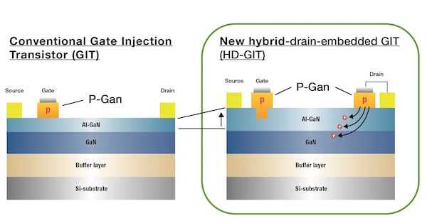
Figure 5. Panasonic’s New HD-GIT in comparison to GIT – Cross Section
Electron trapping and current collapse In the absence of specific technical counter-measures, GaN GiT transistors suffer from electron trapping issues. Generally speaking, these effects are related to the build-up of negative-charged regions in the transistors. This is caused by the trapping of electrons in defects of the crystal and/or at the surface of layers, leading to non-optimal repartition of the electric field in the transistor and disturbing the flow of charge carriers in the 2D gas.
Two trapping effects seem to dominate in GiTs, leading potentially to different destruction mechanisms. Specifically it is understood that the traps contributing most to the build-up of the negative regions are i) deep traps in the buffer layer in the drain to substrate region, appearing under high Vds stress and ii) traps located at the AlGaN surface, capturing hot electrons crossing the AlGaN barriers under hard switching conditions in the semi-on state (Figure 6)
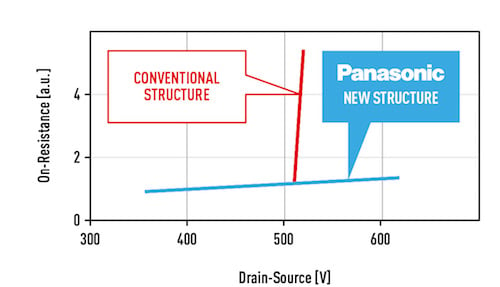
Figure 6. Panasonic’s New HD-GIT in Comparison to GIT – Performance
First consequence: when a drain-source voltage is applied above a certain threshold – dependent on the device characteristics, a bit above 500V for the transistors we are writing about here – the “current collapses”, i.e.from the application point of view the Rds(on) of the transistor increases switching cycle after switching cycle, until it reaches a saturation value. This effect, also known as dynamic Rds(on) typically leads to the rapid destruction of the transistor by thermal breakdown (Figure 6).
Second consequence: the hot electrons captured at the surface of the AlGaN layer in the “semi-on” state under hard switching conditions are suspected to trigger a positive destructive feedback loop that will see the electric field at the drain side increase due to the trapped charges, causing more trapping at the AlGaN surface, causing a further increase of the electric field etc. until the device breaks down.
Panasonic's HD-GiT Structure Solving the Current Collapse
So far Panasonic has been the only provider of GaN components to publicly announce the complete elimination of the problem of current collapse. The figures 5 & 6 shows Panasonic’s unique approach for solving the issue. An additional p-doped structure, similar to the gate, is grown near the drain and electrically connected to it. That structure injects holes into the GaN components, that recombine with the trapped electrons and reduces the maximum electric field in the device, leading to less trapping.
The HD-GiT uses a recessed gate so that the thickness of the AIGaN layer is increased in order to avoid depletion of the charge carriers under the p-doped area close to the drain. The HD-GiT was proven to have the same excellent switching characteristics as the conventional GiT structure. Failure mechanisms in GaN transistors, in general, have been closely investigated in the past decade and discussed in many papers. Let’s now review the most important aspects of Panasonic’s X-GaN transistors’ reliability.
Reliability
In order to guarantee the reliability of the HD-GiT transistors in mass production, Panasonic not only tests against the usual JEDEC standards for Si components but also developed its own additional GaN-specific tests to guarantee the long-term stability of the transistors, for example with regard to current collapse. Accelerated life tests have shown a worst case FiT rate of better than ~10 FIT can already be achieved. Electron trapping and current collapse.
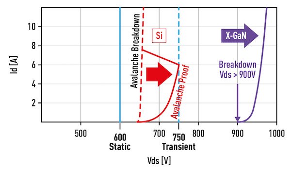
Figure 7. Extra margin on the breakdown voltage
End of Life Test
The end of life mechanism in the GiT transistors seems to be well modeled by a so-called percolation degradation model, where the accumulation of defects over time along the path of leakage currents ultimately creates a conductive path that will cause a time-dependent breakdown. The lifetime of HD-GiT transistors is demonstrated to be related to the p-drain leakage current, by comparing physical models with the Weibull plots of transistors failures under High-Temperature Reverse Bias (HTRB) conditions. According to this understanding, the thickness of the lattice buffer in Panasonic’s X-GaN transistors has been adjusted to limit the p-drain to substrate leakage, aiming to achieve a failure rate over time less than 0.1% for 10 years operation (at Vds=480V and Tj=100°C). Accordingly, the HTRB test is one of the most critical tests to assess the lifetime of the XGaN transistors. It was therefore performed on 10,000 transistors, taken from 20 different lots, far beyond JEDEC requirements. Data corresponding to 1 billion devices and hours equivalent of operation were accumulated. No failures were observed during the test, proving that the said 10 FiT target set by Panasonic as the minimum acceptable level to start the mass production had been achieved.
Robustness in Application
Besides extensive testing of the critical aspects affecting the devices’ intrinsic reliability and lifetime, Panasonic X-GaN transistors also provide robustness by design, contributing to the safe design of application circuits. The first, obvious aspect, lies in the X-GaNs being normally off transistors and appeals no further comments here. There is more, however…
Diode Gate, Doesn’t Break
The gate of the HD-GiT transistors in on state behaves like a diode. This means that there is no breakdown destruction to fear in case of voltage spike on the gate. Gate noise will be clamped by the diode and “absorbed” as transitory peak current.
The safety of the gate circuit is therefore ensured by design. This is a significant advantage as compared with other devices implementing different gate contact concepts, that impose the gate signal to be kept within a very narrow voltage range in on-state, and that is very sensitive to overvoltage breakdown. The benefit comes at a very small cost in the HD-GiT: the small gate injection current drawn by the gate under normal turn-on condition will typically cause gate losses around 10mW, which is neglectable from the point of view of the efficiency of the system.
Extra Margin on the Breakdown Voltage
Unlike MOSFETs, GiT’s lateral structures have no junctions that will avalanche and clamp voltage spikes above the rated breakdown. The GaN material’s wide bandgap property, however, allows the design of small dies with high breakdown voltage. Therefore, to warrantee a failsafe operation of the transistors for example in the event of line surges, Panasonic X-GaN devices have been designed with a with a big margin on the drain-source breakdown limit. Indeed the static field-dependent breakdown voltage of the currently available transistors qualified for 600V operation is in the range of 900V to 1kV (Figure 7). As a side effect, it allows the X-GaN transistors to be qualified with a Vds spike voltage rating of 750V for one microsecond. The vertical field dependent breakdown is also in the same 1kV range; the lattice buffer design (again) is playing here a major role in setting this value.
Panasonic Gate Driver IC
Panasonic brought out its own X-GaN gate driver at the end of 2016 for developers who want to quickly deploy a solution using GiTs. The X-GaN driver IC is optimized for high switching frequencies up to 2 MHz and provides an easy way to unlock the full performance of the transistors. Besides optimized gate control terminals, additional integrated functions are provided – such as a charge pump for (optionally) generating negative gate voltages, or safety features against under-voltage and gate oscillations (Figure 8).
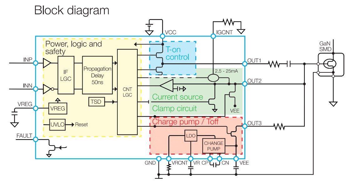
Figure 8. x-GaN gate driver SC
Advantages in Applications
Panasonic’s GiT transistors are aimed at power converters in the ~100W to ~5-6kW range, where MOSFETs with 600V to 650V are typically used today. Depending on the requirements of the application, developers can target maximum efficiency, maximum power density, or a compromise between the two.
Thanks to their “0 reverse recovery” behavior, GaN transistors make some topologies practically usable, such as for example totem-pole PFCs, which require fewer parts as conventional designs and exhibit state-of-the-art efficiency performance. Increased switching frequency enables passive components to be miniaturized – in particular, magnetic components – whereas the power density of circuits such as resonant DC-DC converters can be increased.
Last but not least, GaN brings significant efficiency improvements under partial load operation in resonant circuits of this type Panasonic has used and demonstrated these capabilities in a highly compact and efficient AC-DC demo unit (Figure 9).
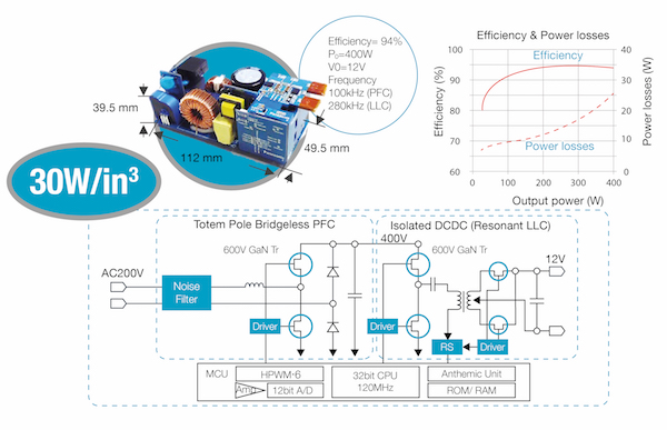
Figure 9. AC-DC demo unit
Applications like power supplies for IT, telecoms servers and AC adapters should benefit the most from these in the short term. The automotive industry has also demonstrated significant interest in being able to use such components in on-board chargers or DC-DCs in the medium term.
About the Author
Francois Perraud is a team leader on power and automotive solutions semiconductor at Panasonic that offers systems and technology focused on making mobility more comfortable, safer and more eco-friendly. From entertainment systems to green energy solutions, Panasonic’s advanced technology and expertise expands the possibilities of future car development. The aim is to be an indispensable partner to European OEMs and key industrial branches for both systems and components. Therefore the company continues to provide significant value and growth potential for customers and drive innovation in the European automotive industry through the ongoing development of solutions for greater safety, energy efficiency and connectivity.
This article originally appeared in the Bodo’s Power Systems magazine.