Facebook
 Google
 GitHub
 Linkedin
Worried About Gate Driver Insulation? Apply the ‘BIER’ Test
This article examines the effects and explains how they can be mitigated along with results of experiments to evaluate stress and damage, particularly partial discharge (PD).
Latest Wide Band Gap (WBG) semiconductors are approaching the ideal with hyper-fast switching at high voltages with low losses while modern MOSFETs and trench IGBTs can also show high dV/dt and di/dt levels. However, fast switching in ‘low-side’ circuits can couple transient voltages to gate drive circuits causing chaotic operation or damage while ‘high-side’ gate drives are additionally subject to stress to their signal and power isolation. This article examines the effects and explains how they can be mitigated along with results of experiments to evaluate stress and damage, particularly partial discharge (PD).
Modern semiconductor switches using Wide Band Gap (WBG) technologies and even MOSFETs and some IGBTs are capable of extremely fast switching. This reduces dissipation during switching transitions allowing higher frequency operation at high efficiency, higher power density, smaller passive components and lower cost. However, there is a downside of increased EMI and stress on gate drive insulation systems due to high dV/dt and di/dt levels.
Figure 1 shows a typical gate drive circuit for an IGBT applying a positive voltage between 5V and 20V to switch the device ON and 0V to switch it OFF. Statically, this circuit also works perfectly well for enhancement mode Si MOSFETs and WBG devices in SiC and GaN technology – in all cases the device is guaranteed to be off with continuous gate 0V applied.

Figure 1: Simplistic gate drive circuit
However, problems occur when the device is switched fast and parasitic capacitive and inductive elements, as shown in Figure 2, come into play.If we take the example of a di/dt figure for drain-source current of 10A/ns, which is feasible with state-of-the-art GaN devices, and a source inductance of 15nH, according to V = - L di/dt, 150V appears across the inductor. On switch-OFF, the voltage drags the source negative, opposing the gate drive and on switch-ON, the direction is positive, again opposing gate drive.
The consequence can be loss of efficiency and even damage due to spurious turn-on causing shoot-through. 15nH may seem large but represents only about 25mm of PCB track. Even a PCB via has an inductance of about 1.2nH producing a 12V transient. In practice at these high di/dt levels, only chip-scale packaging is practical with Kelvin connections to the gate and source for the gate drive. Driving the gate with a negative voltage for the OFF-state helps when some inductance cannot be avoided.

Figure 2: Gate drive with parasitic elements included
In real circuits such as push-pull or full-bridges in inverters or motor control, two low-side devices often share a common return for source and gate drive current as shown in Figure 3.

Figure 3: Low-side devices sharing common grounds
Now Kelvin connections are not possible as there are two drivers, each with their own return. The two driver grounds and two emitter (source) connections must connect together and if this point is, say, physically at Powergnd 1, close to the left-hand switch, the right-hand switch would see more source connection inductance than the left, leading to asymmetrical switching, potential EMI and damage due to induced voltages across the inductance. For symmetry, the point ‘Powergnd 2’ is the only option but is a poor compromise as now both sources have equal but large connection inductances in the gate drive loop, particularly in high power systems where the devices may not be physically close.
A solution is to provide isolated signals and power supplies to the two gate drivers as shown in Figure 4. Now the driver signal and power returns can connect directly to their respective device emitters (sources), excluding most external inductances from the drive loops.
High side switching challenges
The arrangement of Figure 4 solves the problem of di/dt causing gate voltage transients from emitter (source) inductance. It is typically also used for the two ‘high-side’ switches in a ‘H’ bridge where the two gate drive returns are actually anti-phase switching nodes and therefore must be isolated from each other.
In the high-side arrangement, the high switched voltage now appears across the gate drive isolation components and can cause other problems. High dV/dt is the issue with amps of displacement current possible through the isolation capacitance according to I = C dV/dt. With edge rates of 100V/ns easily possible, 10pF barrier capacitance would pass one amp of current, circulating through the primary of the gate drive circuit with potential disruption to operation.

Figure 4: Gate drives incorporating signal and power isolation with Kelvin connections
The gate drive signal isolation components are typically optocouplers or transformers, with capacitor coupling sometimes used. Performance of isolated gate driver ICs is given by the key parameters shown in Table 1 with CMTI, the Common Mode Transient Immunity most relevant to our high dV/dt circuit. However, this value is a laboratory measurement with, most likely, single pulses. Nothing is said about reliability with sustained high voltage, high dV/dt waveforms.

Table 1: Key parameters of isolated gate drivers
Other parameters VIORM/VIOWM/VIOTM/VPR are important, but again are not directly relevant to our switching circuit with standard tests often defined at 50/60Hz, DC or peak values. Separate gate drive transformers have similar limitations to specifications with often just simple ‘Hi-pot’ tests quoted for one second or one minute, typically at some DC level or AC at 50/60Hz. It would be rare to find a rating for reliability at high, switched voltage at high frequency, imposed across the windings or even CMTI.
For transformers, methods of obtaining high insolation vary with the application; enamelled wire-on-wire may stand a single ‘Hi-pot’ test but is not reliable, with almost guaranteed pin-holes in the lacquer. Safety agencies certainly do not allow this as a safety barrier at any voltage. Wire with better insulation such as ‘triple insulated’ types can achieve safety agency approval but is bulky and results in a transformer with relatively high coupling capacitance and displacement current.
The ideal construction is one where windings are physically separated by a guaranteed distance through air to satisfy safety agencies, provide low interwinding capacitance and with no reliance on solid material which could be subject to partial discharge.
The exact same considerations apply to the transformers inside isolated gate drive power supplies with CMTI ratings often omitted and high voltage isolation specified in a variety of ways.
Partial Discharge effects
We have mentioned partial discharge (PD), the slow degradation of solid insulating material subjected to high voltage stress. The effect is caused by sequential break-down of micro-voids in the material which, if an organic type, leads to carbonisation by the plasma produced. The voids become permanent short circuits, reducing the effective overall insulation thickness leading to higher voltage field strength across the remaining insulation and eventual total run-away failure. The PD effect starts abruptly at an ‘inception’ voltage which depends on the gas in the void, pressure and void size and is characterised by the ‘Paschen’ curve [1]. With a switched voltage, the inception point also depends on frequency.

Table 2: ‘BIER’ test configurations

Figure 5: Gate drive transformer with physical separation between windings
Even the breakdown voltage of bulk materials should not be taken at face value. Glass for example, considered to be an excellent insulator, has a breakdown voltage of about 60kV/mm - but this is at 60Hz. At 1MHz the figure is less than one tenth of the value at about 5kV/mm. With some gate drive ICs having quoted distance through insulation of <10μm, high frequency effects need to be carefully considered. Switched voltage levels, dV/dt and frequency are therefore key parameters in the evaluation of insulation re-liability. Transient voltages due to overshoots and resonances with parasitic capacitances and inductances should also be evaluated and added to system voltages.

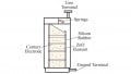
Figure 6: PD test evaluation circuit
Barrier Insulation Evaluation and Research
Gate drive power supply manufacturer RECOM [2] has acknowledged the potential problems with transformers in DC-DC converter products subjected to high, switched common mode voltages and has undertaken a study in conjunction with the insulation materials expert Priv.-Doz. Dipl.-Ing. Dr.techn. Christof Sumereder of Technische Universität Graz and FH Johanneum. The work, internally coded ‘BIER’ (Barrier Insulation Evaluation and Research), comprised of evaluation of 30 half-bridge power stages specially constructed with isolated high and low side switching, Figure 6. Three different configurations were built as in Table 2 and run for 1464 hours at 70°C ambient, a DC rail of 1000V, switching frequency of 50kHz and edge rate of 65kV/μs.

Figure 7: PD evaluation results
T1 was not part of the test
Partial discharge measurements were made before and after the test run showing that in the configurations used, there was no significant deterioration in performance (Figure 7). PD inception voltage remained at over twice the applied peak switching voltage, indicating a good margin and predicting reliable long-term operation. The full report is available from the RECOM website [3].
Conclusion
Isolation of gate driver signals and power in push-pull and bridge circuits solves the problem of voltage transients coupling to the gate in ‘low-side’ and ‘high-side’ circuits. However, the high side isolation components are still subject to high common mode voltage stress at high frequency and high edge rates. Practical partial discharge tests have shown that isolation components in gate driver DC-DC supplies can be designed to have good long-term reliability. RECOM has ranges of DC-DC converters with output voltages and isolation ratings suitable for high-side gate drivers for IGBT, SiC and GaN technologies.
About the Author
Markus Stöger works at RECOM Power GmbH ain Power Electronics Development since August 2015. RECOM products are successful in all areas of electronics - from industrial automation and energy technology over e-mobility, measurement, and railway technology to medical electronics and the Internet of Things.
This article originally appeared in the Bodo’s Power Systems magazine.