 Facebook
 Google
 GitHub
 Linkedin
Gate Driver Failure in High dv/dt Converters
High dv/dt switching can make gate drivers a point of failure. Parasitic coupling and false turn-on may cause unwanted switching and put extra stress on devices.
High-speed, high-voltage converters often face reliability issues. The gate driver is more than just a control interface; it can be a main failure point. In a half-bridge inverter, even a brief parasitic turn-on of less than 100 ns can cause shoot-through currents that go beyond the device's short-circuit rating, damaging both switches in one cycle.
At switching rates of tens or hundreds of kV/µs, parasitic coupling in the gate loop can trigger unintended turn-on events that standard design analysis might overlook. These transient effects are a leading cause of failure and usually appear only during real-world operation, when layout parasitics and system interactions are most important.
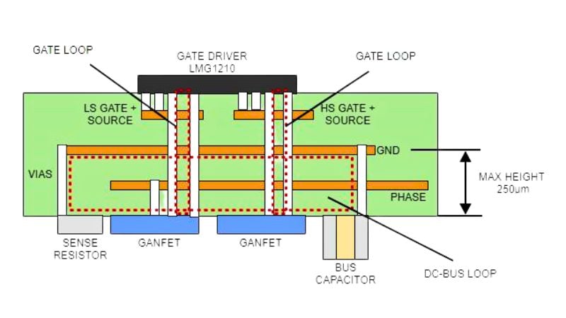
Figure 1. Gate loop vs power loop in a high dv/dt GaN layout. Shared inductance between loops can cause parasitic coupling, false turn-on, and switching stress. Image used courtesy of Texas Instruments
Gate Drivers as Active Failure Initiators
In high-voltage converters, the gate driver does more than pass signals. As switching speeds increase with SiC MOSFETs and fast IGBTs, the gate driver itself can become a failure point. At these speeds, the driver might react to transient coupling rather than the intended signal, especially when dv/dt goes above 50-200 kV/µs. Even a short current spike can push the gate-source voltage (Vgs) close to its threshold.
Two parasitic elements affect the Miller capacitance (Cgd), allowing drain-voltage swings to create unwanted current at the gate.
$$I_{Miller} = C_{gd} \times \frac{dv}{dt}$$
For instance, with Cgd =10 pF and dv/dt= 100 Kv/µs
$$I_{Miller} = (10 \times10^{-12}) ~\times~ (\frac{10 \times10^{3}}{1\times10^{-6}})$$
If this current flows through a 5 Ω gate impedance,
$$V_{gs} = (1 \text{ A}) \times (5 \text{ } \Omega) = 5 \text{ V}$$
A brief gate source voltage spike of about 5 V can reach or go beyond the threshold voltages for many SiC MOSFETs. Even if this pulse lasts only for a few nanoseconds, it can cause false turn-on, and as switching speed increases, managing Miller-induced gate transients becomes more important for reliable gate-driver design.
Another factor is common source inductance (CSI), which adds extra voltage to the gate-source loop during switching transients, making the problem worse.
$$V_{CSI} = L \times \frac{di}{dt}$$
With just 10 nH and di/dt = 500A/µs
$$V_{CSI} = (10 \times 10^{-9}) \times \frac{500}{1 \times 10^{-6}} = 5 \text{ V}$$
Even a small increase in voltage in the gate loop can have a big impact. For a SiC MOSFET with a 4 V threshold voltage, this effect combines with Miller-induced current and ringing, which can push the voltage 1.1 V above the threshold and cause unintended turn-on.
When this effect combines with Miller-induced current and ringing, it can cause unintended turn-on. The key issue is not just one parameter, but how layout inductance, shared paths, and packaging interact during real switching. As dv/dt increases, the gate driver loses full control of Vgs. Failures often begin at the driver interface, not in the device itself.
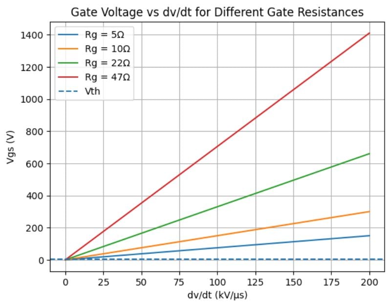
Figure 2. As dv/dt and gate resistance increase, gate voltage rises. This reduces the margin to the threshold, making unintended turn-on more likely. Image used courtesy of Bob Odhiambo
Parasitic Inductance and Gate Loop Instability
CSI adds voltage directly to the gate-source loop during switching transients. Unlike capacitive coupling, this effect depends on the speed of current changes.
$$V = L \times \frac{di}{dt}$$
The induced voltage appears in series with the source terminal, shifting the gate reference point. Even if the driver output stays steady, the device sees a different Vgs. Polarity matters. During turn-on, rising current causes a voltage drop across the source inductance, which lowers the effective gate drive. During turn-off, this effect can raise Vgs, pushing the device toward unintended conduction.
In real systems, CSI is spread across the layout, PCB traces in the source return path, bond wires inside the device, and shared return paths between the gate and power circuits. All of these create shared impedance, which lets switching current enter the gate loop and causes the gate reference voltage to shift as current flows.
Table 1. Typical sources of gate loop inductance in practical layouts.
| Source | Typical Inductance (nH) |
| PCB gate trace (5 cm, 0.5 mm wide) | 15-25 |
| Bond wire (25 µm, 2 mm long) | 2-3 |
| Source pin/package lead | 3-7 |
| Shared power/gate return path | 5-15 |
| Total typical gate loop | 25-50 |
The 10nH in the earlier example assumes ideal conditions. In a real PCB layout, the 5 V caused by CSI should be seen as a minimum, not the worst case. A common solution is to use a Kelvin source, which is a dedicated source pin for the gate return path, kept separate from the power return. By isolating the gate reference from the power current path, the Kelvin source removes shared impedance that allows switching noise to enter the gate loop.
Today, Kelvin source connections are standard in SiC MOSFET packages and power modules. In high-speed designs above 50 kV/µs, they are essential.
Practical Failure Scenarios
Half-Bridge Shoot-Through
In half-bridge setups, a false turn-on of the complementary switch can create a direct path across the DC bus. When the high-side device switches quickly (high dv/dt), parasitic coupling might briefly turn on the low-side device, causing dangerous shoot-through currents that can go beyond safe limits.
SiC MOSFETs can usually handle short circuit currents 6 to 8 times their rated value for 2-10 µs before thermal runaway starts. Any shoot-through lasting longer can cause failure, no matter what the gate control does next. At first, this may look like occasional current spikes, but over time, the extra heat can cause the device to fail completely.
In motor drive systems, long cables act like transmission lines, causing voltage reflections at the motor terminals that increase the effective dv/dt at the inverter output. The size of this reflection depends on the mismatch between the motor and cable impedance.
$$r = \frac{z_{motor} - z_{cable}}{z_{motor} + z_{cable}}$$
For example, if the motor is 400 Ω and the cable is 50 Ω, then r = 0.78. This means the reflected wave adds 78% of the original voltage, almost doubling the dv/dt at the motor terminal and sending it back to the inverter gate circuits, which can trigger unintended turn-on. Systems that seem stable with short cables might fail in real use with longer cables.
In parallel switching setups, even small layout or packaging differences can cause mismatched parasitic inductance and capacitance, leading to uneven switching times. A small 0.5 V gate threshold difference between two parallel SiC devices, along with a 5 nH difference in source inductance, can cause one device to carry 30-40% more current during switching. This ongoing imbalance can cause the overstressed device to fail early.
Failure Signatures and Diagnostics
A clear sign of a gate driver failure is random turn-on events, in which the power module activates without a gate signal during high dv/dt transitions of the complementary switch. These events depend on the load and happen occasionally, making them hard to reproduce in static tests.
Another symptom is local overheating, often in half-bridge or parallel setups. A steady load imbalance does not cause this, but by brief transient events. Partial unintended turn-on can also increase switching losses, causing more current overlap and higher losses even when control signals stay the same.
Probing Vgs Correctly Under High dv/dt
To measure Vgs accurately under high dv/dt conditions, you need a careful probe setup. A standard probe with long ground leads acts as an inductive loop, picking up switching noise and creating false ringing that looks like gate spikes.
To avoid this, place the probe directly across the gate and source using a coaxial tip or spring ground to keep the loop area small. Make sure the probe has at least 500 MHz bandwidth so fast edges are not distorted, and always measure between gate and source to prevent common-mode noise from affecting the waveform.
The best way to find these problems is to measure the gate-source voltage with high-bandwidth equipment. Watch for voltage spikes on Vgs when the complementary device switches. If these spikes do not show up at the driver output, they are parasitic. Also, look for high-frequency ringing above the threshold voltage (Vth), since even short peaks can cause problems. Good probing methods make these effects easier to see, while poor probe grounding can hide or distort them.
Defining Safe dv/dt Operating Limits
One practical way to check for false turn-on risk is to calculate the highest dv/dt that keeps the induced gate voltage below the threshold voltage, using the earlier formula.
$$(\frac{dv}{dt})_{max} = \frac{V_{th}}{C_{gd} \times R_g}$$
This formula sets an important limit: If dv/dt increases, the Miller-induced gate voltage can trigger unwanted conduction. These calculated limits are often much lower than what you see in real operating conditions.
For example, with Vth = 4 V, Cgd = 150 pF, and Rg = 10 Ω, the maximum dv/dt is about 2.67 kV/µs. But SiC converters usually run at 50 to 200 kV/µs, which is much higher. The formula only covers Miller coupling, but real systems also have effects from common source inductance and ringing, making the safety margin even smaller.
Using a negative bias raises the voltage threshold that the parasitic coupling must overcome to trigger an unintended turn-on, effectively making noise work harder to activate the device. This boosts the maximum allowable dv/dt, as shown in the formula.
$$(\frac{dv}{dt})_{max} = \frac{V_{th} - V_{gs,off}}{C_{gd} \times R_g}$$
With -5 V off-state bias, the safe dv/dt increases to about 6 kV/µs, which is more than double what you get at 0V. However, this is still below typical SiC switching speeds, so negative bias must be combined with good layout and proper gate drive design to fully manage parasitic effects.
Where Failure Begins
Dv/dt-induced gate errors are often the first sign of trouble. The fast transients that cause false turn-on do not stay in one place; they spread through the entire gate driver. Over time, these repeated high-field transients slowly wear down the isolation barrier, even if voltages stay within rated limits. Damage builds up quietly until failure happens.
This shifts the focus from switching performance to how well the insulation holds up, and raises the key question: Can the isolation barrier handle ongoing transient stress from high dv/dt operation over the product's full lifetime?


The example of a 0.5mm side trace (only 20 mil) for a high-current gate drive is not “typical” but, we get the point. Yes, paying attention to parasitics is extremely important for high dV/dt and di/dt. Experienced power electronics engineers who actually calculate the many details such as trace inductance are needed to avoid such errors. We also have ways to reduce the effect of parasitics using circuits such as active and passive snubbers and proprietary switching techniques.