Facebook
 Google
 GitHub
 Linkedin
Understanding Bandwidth Requirements When Measuring Switching Characteristics
With the advent of wide bandgap semiconductors, we are facing a transition to higher operating frequencies and more importantly shorter switching times.
This transition is asking for measurement setups with higher bandwidth. However, it also places more emphasis on the question, “Which bandwidth is good enough for doing the job?”
In a previous article, “Overcoming Challenges Characterizing High Speed Power Semiconductors” [1], Keysight had a general look into the bandwidth required for Double Pulse Test Systems. In that article, we discussed bandwidth, but with a focus on the requirement for the Double Plus Test (DPT) circuit design. We highlighted how there are different contributors to the overall system performance. In this article, we are focusing on the aspect of measuring and bandwidths that are required for specific signals.

Figure 1. Switching transition and its properties.
This article proposes a method for estimating the required measurement bandwidth. Two aspects must be considered: 1) the properties of the signals to be measured, and 2) the properties of the measurement setup (i.e. oscilloscope) itself. Both aspects will be discussed to estimate the bandwidth requirements needed for measuring switching characteristics in power electronic applications accurately.
Signal Properties
A signal has many different properties which determine the measurement requirements, for instance, the ‘signal levels’ to be measured. The discussion in this article focuses on the properties dictating the bandwidth requirements.

Figure 2. Simulated rising edges (limited transition time vs. ideal edge)
The bandwidth requirements are determined by two properties:
- Transition times: The times it takes for a signal (e.g. VDS) to switch from high to low or vice versa, when a transistor is turned on or off. It is not the switching frequency of the transistors that determine the bandwidth requirements, but the transition times.
- Ringing: There are always parasitic capacitance and inductance present in each circuit, forming LC circuits. When a transistor is switching, those LC-circuits become excited and start to oscillate. The oscillations are damped by resistive elements in the circuit and therefore fade away after some time.
Properties of Transition Times
In power electronics transistors operate as switches. They are either turned on, or off, or are transitioning between both states. Ideally, the transitions are as fast as possible to minimize switching losses. The characteristic of switching on and off is also a common theme in digital design, where one is mainly measuring and analyzing square wave signals.
In the book “High-Speed Digital Design – A Handbook to Black Magic” [2] Howard W. Jonson and Martin Graham are describing a method for estimating the maximum frequency up to which a digital signal contains significant amount of energy. Using a simulated example, we would like to introduce this approach here.
To start the discussion, we compare the signal spectrum of an ideal square wave (V2 - blue) with a waveform showing a realistic transition time (V1 - red) (see Figure 2).
V1 has a 10%-90% transition time of about 1.8ns. The markers highlight when the signal is crossing the 10% threshold (m1) and the 90% threshold (m2). V2 has an almost ideal transition time (i.e. time ~ 0 ns). Calculating the respective spectrums yields the following results (Figure 3).
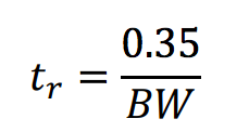
The ideal spectrum of V2 (blue) shows a decline of 20dB/decade. However, the spectrum of V1 (red) starts to roll off at a certain frequency. The frequency at which the amplitude has dropped by half (6dB), compared to the ideal spectrum is labeled “knee frequency” Fknee [2]. In this example Fknee happens to be 278MHz. We can relate Fknee and the 10%-90% transition time (tr ) and end up with this easy-to-remember formula:
Of course, the same formula also applies for fall times (tf ).
To summarize, using this formula, we can estimate to which frequency a square wave signal carries the significant amount of energy, given its rise or fall times. If we want to be able to accurately measure this signal, we must make sure we capture all frequency components up to this knee frequency – plus some headroom. The amount of headroom required is the topic of the following section.
Properties of Ringing
As already mentioned above, power electronic circuits contain parasitic components forming a LC-circuits, which becomes excited when there is a switching event. When it comes to estimating the required bandwidth for capturing the caused ringing, we can focus on the highest frequency oscillations of the signal only. The highest frequency oscillations are mainly created by the combination of the power loop inductance Lloop and the output capacitances Coss of the transistor.
The schematic below (Figure 4) shows both using a typical double pulse test configuration as an example.
Knowledge of these parasitics allows us to estimate the resulting oscillation frequency, using this formula calculating the resonant frequency of an LC-circuit:
Coss can be found in the data sheet of the transistor. However, strictly speaking, it is not the only contributor. Other parasitic capacitances must be considered as well. They typically are in parallel with Coss and just add onto Coss, increasing the parasitic capacitance value. If one neglects these additional capacitances, the estimate of the ringing frequency will result in a slightly higher value. It is also not straightforward to determine Lloop. You might use suitable circuit simulations or measurement techniques (shown later in this article). to estimate its value. If you underestimate the actual value of the loop inductance, you will estimate the bandwidth requirement a little bit too high, which provides extra margin in your measurement design.

Figure 3. Extracted spectrum (limited transition time vs. ideal edge).
Figure 4. Main contributing parasitics to high-frequency ringing in DPT system.
Oscilloscope Properties
When you combine many circuit elements with similar frequency responses, you get a Gaussian response. Traditional analog oscilloscopes chain many analog amplifiers from the input to the cathode ray tube (CRT) display and therefore exhibit a Gaussian response.
Less familiar, is probably the flat response that is now more commonly exhibited by modern, high-bandwidth digital oscilloscopes. A digital oscilloscope has a shorter chain of analog amplifiers, and it can use digital signal processing techniques to optimize the response for accuracy. More importantly, a digital oscilloscope can be subject to sampling alias errors which is not an issue with analog scopes. Compared to a Gaussian response, a flat-response reduces sample alias errors, an important requirement in the design and operation of a digital oscilloscope.
The topic of how the frequency response and the oscilloscope’s system bandwidth effect the measurement results is described in more detail in the Application Note “Understanding Oscilloscope Frequency Response and Its Effect on Rise-Time Accuracy” [3] by Keysight Technologies. Here we are summarizing the key takeaways.
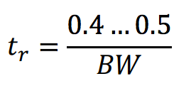
For an oscilloscope with gaussian frequency response, the intrinsic rise time of the step response can be calculated in the following formula:
For oscilloscopes with flat frequency response there are more variations of equations. But in general, its rise time of the step response can be estimated to be the following:
Nevetheless, you can’t simply assume that an oscilloscope with Gaussian frequency response yields results with higher accuracy when it comes to measurement of transition time. On the contrary, using an oscilloscope with a flat response with a sufficiently high bandwidth margin yields better results. The bandwidth in equations 3 and 4 is referring to the system bandwidth. You might have come across the following formula for calculating the system bandwidth from the oscilloscope’s bandwidth and the probe’s bandwidth.

Determining How Much Bandwidth You Need
Bandwidth requirements being imposed by Transition Times In a previous section, we’ve learned how to estimate up to which frequency (Fknee) a signal carries significant energy based on its transition time. We’ve also learned that oscilloscopes might show different types of frequency responses on their input and this must be considered when estimating when choosing the amount of required bandwidth. The missing piece of information is how much margin should be between the knee frequency and the oscilloscope’s bandwidth. For this, no formulas are available. However, the application note mentioned in the previous section [3] lists some evaluation results down to a practical limit with an accuracy of 3%.
Table 1. Required Bandwidths
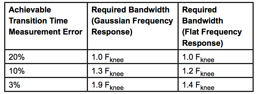
Therefore, to estimate the required bandwidth given a certain 10%- 90% rise time, you should follow these steps:
1. Determine the knee frequency using Fknee=0.5/tr.
2. Determine the frequency response of your oscilloscope (either gaussian response or flat response).
3. Based on the type or oscilloscope, pick the corresponding multiplier from the table above (e.g. for flat-response and 3% of error → 1.4). 4. Calculate the required bandwidth using this multiplier at Fknee.
This procedure is only a tool to estimate the bandwidth you need. It is prudent to verify actual rise-time accuracy with measurements, as frequency responses vary between oscilloscope models.
Finally, you should make sure that the sampling rate is set sufficiently high. Again, we are referring to Keysight’s application note [3]. The application note provides a guideline of how to derive a sufficiently high sample rate from the system bandwidth.
1. For an oscilloscope with gaussian frequency response a sample rate at least 4 times higher than the system bandwidth should be used.
2. For an oscilloscope with the flat-frequency response, a factor of 2.5 between bandwidth and sample rate is sufficient.
Bandwidth Requirements Being Imposed by Ringing
As described above for estimating the maximum frequency to expect in the ringing we should understand the expected parasitic capacitances and inductances in the circuit. As previously discussed, for the capacitances we can use the value of Coss. One way to determine the approximate Lloop is to extract the value from measurement results. We can look at the transitions of VDS (red) and IS (green) of a turn-on event as shown in Figure 5.

Figure 5. Extraction of power loop inductance.
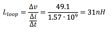
We notice there is a dip in the voltage when the current is rising. This is caused by the loop inductance and is mathematically expressed as the following.
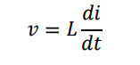
The voltage (v) corresponds to the height of this voltage dip ∆u, highlighted by markers M3 and M4 (I.e. 49.1V). The derivative di/dt can be determined by measuring the change in current (∆i) over a time period (∆t), as highlighted by the markers M1 and M2 (I.e. 1.57Ga/s). Note - this is the initial slope when the dip reached its maximum height.
With this information, the loop inductance can be estimated as follows.
With this estimate of Lloop and Coss the frequency of the ringing can be estimated, as previously described above (Equation 2).
Examples
Now it’s time to test the rule of thumb being introduced in the previous section in practice.
Analysis of Transition Time
The following measurements have been taken with the PD1500A Dynamic Power Device Analyzer/Double Pulse Tester. This system is using a DSOS104A sampling oscilloscope in conjunction with the 10076C high voltage single ended probe for measuring VDS. This combination provides a system bandwidth of 500MHz. The filter characteristic of the oscilloscope is a flat-frequency response.
The SCT2080KE SiC power MOSET from Rohm Semiconductors was chosen as the DUT. Its maximum operations conditions are1.2kV and a current up to 40A. The measurement conditions to measure rise time and fall time are specified in the transistor data sheet. The only difference between the data sheet test conditions and the PD1500A test conditions is that the data sheets specify a resistive load and the double pulse test system uses an inductive load.
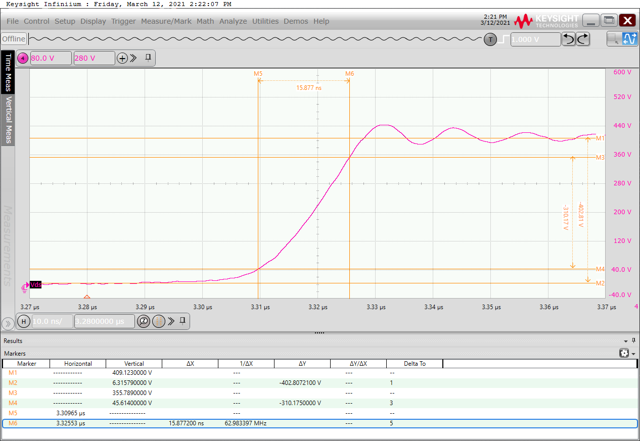
Figure 6. Rise time measurement with 500MHz bandwidth.
The “fall time” in the data sheet is given as 22ns. With the PD1500A we measured 15.9ns. However, since we don’t have the identical measurement conditions (i.e. inductive load instead of a resistive load), the difference may not be a concern. We have discussed correlation situation in more detail in the previous article, “Designing a Double-Pulse Test (DPT) System to Enable Correlation of Dynamic Characteristics" [4].
Nevertheless, this is a good indicator, the fall time was measured correctly, and therefore we used a sufficiently high bandwidth. With this confirmation, we can now calculate the estimate of the required bandwidth for measuring this transition with an accuracy of 3%.

Figure 7. Rise time measurement with reduced bandwidth.
Forty-four MHz is a surprisingly low bandwidth. So, let us confirm our findings. We can use the feature of the oscilloscope to limit its system bandwidth and set it to 44MHz. This screen shot in Figure 7 shows the measurement result.
As you can see, we’ve still measured the same rise time as before (i.e. 15.9 ns), even though we could have expected a 3% deviation from this value. You can also see that there is a significant change in the signal waveform, specifically in the amount of ringing. Please keep in mind this method is only an estimate.
Analysis of Ringing
For estimating the frequency of the ringing, we must know the output capacitance Coss and have an estimate of the loop inductance Lloop of our measurement system. For this example, we again use the SCT2080KE SiC power MOSET from Rohm Semiconductors. In its data sheet, Coss is specified to be 77pF. The measurement shown in Figure 8 has also been completed with the same double pulse test system used in the extraction in Figure 5, so we will use the estimate for Lloop to be 31nH (see equation 7). Using results and Equation 2, we end up with a required bandwidth for the ringing of 103MHz. Putting this estimate to the test, we measured the ringing on VDS after the turn off event using the maximum available bandwidth of the oscilloscope (500MHz). The markers M1 and M2 were placed on the second and third maxima of the ringing. You might have noticed that the ringing doesn’t consists of a clean sine wave. There is distortion in the sine wave indicating some harmonics. Consequently, using the markers in such a way is not the most accurate way to measure the fundamental frequency. Nevertheless, it is good enough for our purposes here and shows us a frequency of about 80MHz. As expected, this is lower than our estimate.

Figure 8: Measurement of ringing with 500MHz of bandwidth.

Figure 9: Measurement of rise time with reduced bandwidth.
Markers M3 and M4 allow us to extract the initial amplitude of the ringing not taking the overshoot into account. approximately 41V. If we followed our initial estimate, we would have done this measurement with just a bandwidth of 100MHz. So, let’s limit the bandwidth of the oscilloscope and see what result we get (Figure 9). By examining the waveforms, we notice the ringing appears much less distorted than in Figure 8. This can be explained by the fact that the harmonics causing those distortions have now been filtered. Checking on the fundamental frequency (again using markers) results in 83MHz and the amplitude reading is now 40V. The discrepancy in the frequency between Figure 8 and Figure 9 can be explained by the simple method we used for measuring frequency. You also notice that the drop in voltage amplitude is only 0.2dB.
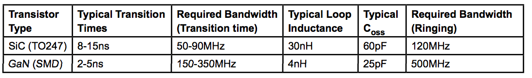
Typical Bandwidth Requirements when characterizing SiC or GaN transistors
Conclusions
When making measurements in power electronics it is important to know the measurement bandwidth required for accurately capturing the signal waveforms. In this article, we wanted to highlight that there are two different signal parameters driving the bandwidth requirements: 1) transition times and 2) ringing frequencies. For both parameters, we have introduced a way to estimate the required bandwidth.
Based on our experience with typical parameters for SiC and GaN transistors, the following table (Table 4) gives an indication regarding the bandwidth requirements you might face for different device technologies. Plus, with the methods we have introduced above, you should be able to adjust these estimates to your specific application needs.
References
1. Overcoming Challenges Characterizing High Speed Power Semiconductors, Bodo’s Power Systems, April 2020.
2. Johnson, Howard and Martin Graham, High-Speed Digital Design: A Handbook of Black Magic, Prentice Hall, 1993.
3. Effect of Oscilloscope Frequency Response on Rise-Time Accuracy: Understanding Oscilloscope Frequency Response and Its Effect on Rise-Time Accuracy, Application Note, Keysight Technologies.
4. Designing a Double-Pulse Test (DPT) System to Enable Correlation of Dynamic Characteristics, Bodo’s Power Systems, August 2020.
Related Content