Facebook
 Google
 GitHub
 Linkedin
Understanding Probing Requirements When Measuring Dynamic Power Module Parameters
For high-quality characterization, wide-bandgap (WBG) transistors need to be characterized dynamically. In contrast to discrete devices, testing a power module in a double-pulse test system requires measuring low-side and high-side signals. This introduces new challenges for isolation and common-mode (CM) rejection due to the high voltage and fast switching. This article provides an overview of the probing requirements for each of the relevant signals.
A dynamic power device analyzer, such as a double-pulse test system, is used to measure the dynamic characteristics of power transistors or diodes. In such a system, it is necessary to measure VDS, VGS, ID and IG as shown in Figure 1 with an oscilloscope. For discrete devices, the measurement requirements can be simplified by placing the device under test (DUT) on the low-side of the half-bridge. This introduces relatively low CM signals. ID can be measured directly with a high-bandwidth shunt.
In contrast to discrete devices, power modules usually contain at least one half-bridge. It is not built symmetrically, which results in different dynamic behavior of the low-side and the high-side. This makes it necessary to also measure VDS, VGS (and ID, IG) dynamically for both low- and high-side.
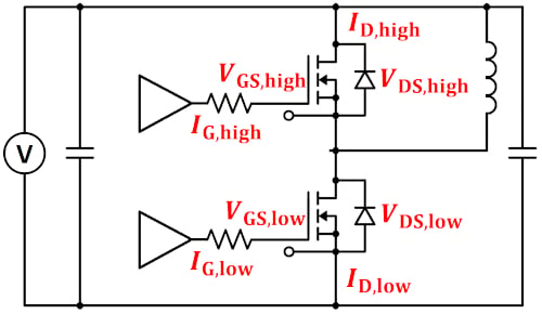
Figure 1. Double-Pulse test schematic with probed signals. Image used courtesy of Bodo’s Power Systems
It is possible to apply the ground potential at the switching node instead of the source potential of the low-side transistor so the requirements for the high-side measurement correspond to those for the low-side measurement. However, it is advantageous to measure both stages simultaneously. This alternative method is therefore not discussed in this article.
Measuring high-side signals is more difficult than measuring low-side signals. In the next section, the requirements will be compared.
Overview of Probing Requirements
The requirements refer to a 1.7 kV SiC module tested at a maximum of 80 % of rated voltage (1.36 kV) with test currents up to 1000 A.
Bandwidth
A transistor with a transition time of 8 ns requires a bandwidth (BW) of 90 MHz. For ringing measurements with a typical loop inductance of 30 nH and output capacitance of 60 pF, the required BW is 120 MHz. The required BW excludes Rogowski Coils and Pearson probes for current measurements.
Isolation
The isolation requirements for low-side measurements are not very strict. The shunt is typically at ground potential. Consequently, when measuring a 4-pin transistor, voltage spikes occur between the Kelvin sense and source pins during switching operations. VDS and VGS are measured with respect to Kelvin sense, which requires some isolation. The voltage spikes are typically in the range of 10 V to 50 V and can be calculated based on the source inductance LS and the current slew rate \(\frac{di}{dt}\):
\[V=L_{S}\cdot\frac{di}{dt}\]
The isolation requirements for high-side measurements are much more stringent. During the test, the high-side signals may be near the ground potential, but they may also be at the supply voltage. Therefore, in this example, the isolation requirements are at least 1.36 kV. With respect to ringing, a margin of 30 % is appropriate. This results in an insulation requirement of 1.8 kV for all high-side measurements. Higher values are required for higher test voltages.
Common Mode Range
Common mode (CM) requirements are similar to isolation requirements. For low side signals, except for, the CM transient is typically in the 10 V to 50 V range. In terms of CM range, high-side signals can be divided into two groups. The first group consists of VDS and ID. For these signals, the requirements are not high because these signals can be measured with reference to the drain potential of the high-side transistor. A well-designed system has a large bulk capacitance, making the supply voltage very stable. Small changes, as 5 % (68 V in this example) of the supply voltage occur very slowly (e. g. within 50 µs) during the pulse.
The second group of high-side signals is the gate signals. These signals are referenced to the Kelvin sense or source pin of the high-side transistor. These pins are located at the switching node, so the voltage change is approximately the same as the supply voltage. The change is very fast during the transition time, for example, 1.36 kV within 10 ns, which is a major challenge in terms of measurement quality.
Common Mode Rejection Ratio
For a voltage measurement, the differential voltage should be measured. However, the CM signal also leads to an interfering measurement signal. The unwanted voltages due to CM signals can be calculated very easily for different CM suppression ratios, see Table 1. It is important to note that the CMRR of probes strongly depends on the frequency. In general, the common mode rejection ratio (CMRR) decreases with frequency.
|
Signal/CMRR |
20 dB |
30 dB |
40 dB |
50 dB |
60 dB |
70 dB |
80 dB |
90 dB |
100 dB |
|
10 V |
1 V |
0.3 V |
0.1 V |
0.03 V |
0.01 V |
3 mV |
1 mV |
0.3 mV |
0.1 mV |
|
50 V |
5 V |
1.6 V |
0.5 V |
0.16 V |
0.05 V |
16 mV |
5 mV |
1.6 mV |
0.5 mV |
|
100 V |
10 V |
3.2 V |
1 V |
0.32 V |
0.1 V |
32 mV |
10 mV |
3.2 mV |
1 mV |
|
1000 V |
100 V |
31.6 V |
10 V |
3.16 V |
1 V |
316 mV |
100 mV |
31.6 mV |
10 mV |
|
1360 V |
136 V |
43.0 V |
13.6 V |
4.30 V |
1.36 V |
430 mV |
136 mV |
43.0 mV |
13.6 mV |
Table 1. Measured voltage by CM signals for multiple CMRRs.
The CMRR of the probe must be high enough over the frequency range where the CM is introduced.
As already mentioned, the CM voltages of the low-side signals are small (e. g. 50 V) and only occur at switching transitions. For low side measurement with shunt, no CM is introduced. For the other signals, the influence measured by CM is ideally smaller than the effective resolution of the measurement system. For gate signals, a typical measurement range is 40 V and with a target value of 10 bits, the resolution would be 39 mV. The table shows that about 60 dB is sufficient. For the measured signal and thus the range is much larger, e. g., 1.8 kV, resulting in a resolution of 1.76 V. A CMRR of 30 dB is sufficient. For both low-side signals, the CM signal has high-frequency components which makes it necessary to have high CMRR over a large frequency spectrum.
For high-side signals, the situation is again more complicated. For the first group of signals which can be referenced to the drain potential, the CM signal is small. A CMRR of 40 dB is sufficient for VDS. ID usually results in only very small voltages measured by the oscilloscope, about 500 mV to 5 V. Therefore, the CMRR requirements are more stringent. Using the same effective number of bits (ENOB) as before results in a CMRR requirement of 100 dB. Note that for both VDS and ID, the CMRR requirement is only for lower frequencies such as 1 MHz.
The high-side gate signals are generally the most difficult to measure in terms of CMRR. In this case, the CM is the supply voltage with high-frequency components and the measurement range is typically only 40 V. This results in a resolution of 36.5 mV and therefore >90 dB is ideal for a wide frequency range.
Note that higher CMRRs than mentioned do not lead to higher measurement accuracies.
Noise
Noise performance is the weak point of most commercial high CMRR probes. In general, the lower the noise, the better. This is especially true for ID measurements since the measured voltage is very small. The shunt value should be chosen as small as possible to minimize circuit influence, but there is a lower limit due to noise. Single digit mV rms values are good. For VDS, noise is not a problem since common high-voltage differential probes can be used and noise requirements are low. Gate signals are typically in between, with a typical measurement range of 40 V. An important parameter is 10 % gate-voltage-time, and with 20 V VGS, one must be able to measure 2 V very accurately. The noise must be much smaller than the measured voltage, so <30 mV rms is ideal. Commercial high-CMRR probes introduce noise of around 200 mV rms for such a range, which makes finding the correct timing difficult. Figure 2 compares noise performance between a commercial high-CMRR probe and the low noise high-CMRR solution.
|
|
BW |
Isolation voltage |
CM Range |
CMRR |
CM frequency |
Noise |
|
VDS,low |
>120 MHz |
50 V |
50 V |
30 dB |
<100 MHz |
1 V |
|
ID,low |
0 V |
--- |
--- |
--- |
3 mV |
|
|
VGS,low |
50 V |
50 V |
60 dB |
<100 MHz |
30 mV |
|
|
I/G,low |
50 V |
50 V |
60 dB |
<100 MHz |
30 mV |
|
|
VDS,high |
1.8 kV |
65 V |
40 dB |
<1 MHz |
1 V |
|
|
ID,high |
65 V |
100 dB |
<1 MHz |
3 mV |
||
|
VGS,high |
1.36 kV |
90 dB |
<100 MHz |
30 mV |
||
|
IG,high |
1.36 kV |
90 dB |
<100 MHz |
30 mV |
Table 2. Summary of probe requirements.
Probe Load
The capacitive probe load must be so small that the measured signal is not significantly affected. A typical SiC transistor has an input capacitance in the single-digit nF range and output capacitance of about 100 pF. Therefore, the load requirements for VDS (single-digit pF) are more stringent than for VGS (double-digit pF is acceptable).
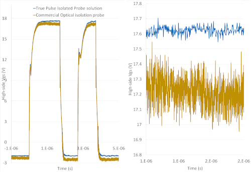
Figure 2. Noise comparison of a commercial probe (yellow) and the True Pulse Isolated Probe solution (blue). Image used courtesy of Bodo’s Power Systems
Table 2 shows the probe requirements for measuring a 1.7 kV SiC module.
Conclusion
High-side probing introduces new problems for a dynamic power device analyzer. is the least problematic of the signals, as the requirements can be met by high-end high-voltage differential probes such as Keysight’s DP0001A. This probe cannot be used as the noise requirements are very strict. Commercial Rogowski Coils or Pearson probes do not fulfill the BW requirements. The stringent requirements for gate signals like high CMRR requirements over a large frequency range and strict noise requirements are not met by commercial probes. In Keysight’s PD1550A a True Pulse Isolated Probe solution is introduced to meet both low-noise and high-CMRR requirements while maintaining isolation and BW requirements.
This article originally appeared in Bodo’s Power Systems magazine.