Facebook
 Google
 GitHub
 Linkedin
Troubleshooting 9 Common DC-DC Buck Converter Issues
Switch-mode, low-voltage, DC-DC, single-phase, non-isolated, basic buck converter circuits don't always work as planned. This article helps troubleshoot nine common issues.
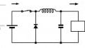
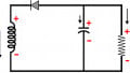
This article addresses troubleshooting a staple of electronic systems that don’t always work as planned: switch-mode, low-voltage, DC-DC, single-phase, non-isolated, basic buck converter circuits.
General Rules for Converter Troubleshooting
When troubleshooting, it’s important to consider the variables and reduce the possible causes of failure.
Here are some guidelines:
- You must reliably make the system fail to troubleshoot it. A problem that goes away by itself comes back by itself.
- Change only one thing at a time and note the effect.
- If the circuit stops working, ask, “what changed?” Was there an event that coincided with the failure?
- See if the failure moves with the converter board, the chip, or the load.
Keeping these guidelines in mind, here are nine common issues you may encounter when designing a DC-DC buck converter and some likely causes.

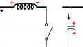
A 10× probe measuring output voltage. Image by Eric Bogatin
Problem #1: Too Much Ripple
If you see too much ripple, the inductance might be too low—higher values give lower ripple but a slower transient response.
Also, keep in mind large inductor ripple current means higher peak currents and a greater likelihood of inductor saturation, especially at high temp—and more stress on your FETs.
Other problems could be Cout too low (not enough storage to hold up the output) or Cout ESR (equivalent series resistance) too high (causing IR drop in Cout).
Finally, low switching frequency will cause more ripple.

Measured noise with a 10× probe. Screenshot by Eric Bogatin from “How to Measure Noise in Switch-Mode Power Supplies (SMPSs)”
Problem #2: Failure To Start
First, ask yourself: Is the “enable” pin driven (or pulled up) correctly? Same for the power good output.
Failure to start up may occur because excessive load capacitance (like for an FPGA) is acting like a short and triggering the current limit. Some chips have blanking and soft-start features to overcome this.
To avoid false alarms, set the current limit point as high as practicable and negotiate with the FPGA engineer to optimize the capacitance on the system level.
Finally, ensure the Vin is not sagging and the UV lockout is not activating due to input droop.
Problem #3: Voltage Present at Output When Off
If your circuit is indeed off but you see a voltage on the output, it is usually coming from another power circuit. Check for non-obvious paths to other active rails.
Problem #4: Bad Regulation
With remote Vout sensing, bad regulation can be caused by power path ohmic voltage drop, maybe due to a rail (single power-converter output line), that is distributed to too many loads on a board. This is why sometimes multi-rail converter ICs (“PMICs”) are avoided in favor of multiple converters next to their loads.
If your voltage sense pin is noisy, keep this pin’s layout clean and make sure any resistors associated with the sense signal are placed near the controller.
Another explanation is that your reference voltage may be unstable on under-filtered.
Problem #5: Slow Transient Response
The primary culprit here is that there may be too much bulk output capacitance or too big an inductor.
Another issue may be bad loop compensation. Loop characteristics are hard to completely characterize without the right equipment. But even if you don’t have a network analyzer, you can use a step load and observe the transient ringing—it will tell you a lot cheaply.
Also, in development, the compensation usually must change if the design load changes. For example, are you using a factory evaluation module at half of its designed-for load? You see the problem.
Problem #6: Instability
Cout ESR can be a cause of instability as it introduces a zero in the loop response, which makes the gain curve stop descending and start going sideways, eroding or eliminating the gain margins. If the zero is low frequency enough, the gain will not pass zero before the phase goes to 180°.
Cheaper converter chips may be internally compensated to save external parts, but make sure your Cout meets the min and max Cout ESR range in which they will be stable.
Other explanations for instability may include bad voltage sense or summing node layout or noise.
Be sure to generate a Bode plot with the design software and check the phase and gain margins, including over temperature.
Problem #7: Low Efficiency
The bootstrap capacitor needs to be big enough to provide charge to the high-side FET gate—otherwise, that FET might not fully turn on and then will burn power. A resistor in series with the boost pin can be used to tune the turn-on to control ringing.
Measuring power circuit efficiency (especially above 90%) is not trivial as it requires current measurements and is the ratio of two power quantities. Hopefully, you have characterized each component’s contribution to the losses via a spreadsheet tool, which will usually tell you that the MOSFETs and the inductor resistance (DCR or direct current resistance) are the main contributors to wasted heat.

A plot showing efficiency vs frequency for a step-down switching regulator. Plot taken from the datasheet for the LT8610 from Linear Tech/Analog Devices.
Problem #8: Low-Temperature
Remember that ESR rises for electrolytic caps at low temperatures, and capacitance falls.
Problem #9: PMBus Issues
On a shared data communication bus, ensure that another node is not intermittently chattering when you are not looking.
Also, ensure that the pullups you’ve used are strong enough: 47 kΩ pullups (like in an FPGA) aren’t nearly as good as 10 kΩ.
Data, Data, Data
If you are at a total loss as to what to do, get more data—that will give you something to analyze, generate ideas, and prompt team discussion.