Facebook
 Google
 GitHub
 Linkedin
Sophisticated Designs for Low-Power DC/DC Converters
Converting one DC voltage to another in an electronic circuit has a history that demonstrates over fifty years of increasing sophistication - modern designs having incredibly high-power densities along with corresponding advances in efficiency to keep the power dissipation low. RECOM’s current designs include many innovations that apply design techniques from high-power power supplies to benefit low-wattage converters in the smallest packages.
This article is published by EE Power as part of an exclusive digital content partnership with Bodo’s Power Systems.
The first DC/DC conversion solutions were all low-noise linear designs that were simple to use but had two major drawbacks. First, the output voltage must always be lower than the input voltage; however, a linear regulator is very inefficient and dissipates a substantial proportion of the supplied power as heat. Second, depending on the voltage difference between input and output, linear regulator efficiencies can be 60% or lower.

Image used courtesy of Adobe Stock
The invention of the switching DC/DC converter solved both problems but required a more complex design methodology. In contrast to linear designs, switching converters exploit the energy-storing properties of inductive and capacitive components to transfer power in discrete packets. The pulses of power are stored either in an inductor’s magnetic field or in a capacitor’s electric field.
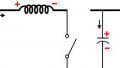
The switching controller ensures that only the power required by the load is transferred in each switching cycle, making this topology very efficient. The best designs can achieve efficiencies of 97% or greater. Figure 1 shows the simplified block diagram of a switching DC/DC converter.

Figure 1. Simplified block diagram of a switching regulator. Image used courtesy of Bodo’s Power Systems [PDF]
The switch function in Figure 1 is performed by power transistors that alternate between their highly efficient “on” and “off” states in a controlled sequence. This contrasts the continuous operation in a linear design. A switching DC/DC converter can produce an output that is either higher or lower than the input (step up or step down) or invert the voltage from input to output.
The output can be either regulated or unregulated. The output voltage of an unregulated converter changes significantly with variations in the load current or input voltage. In a regulated design, a feedback control loop (dotted line) feeds the output voltage back to the switching block; this changes the switching operation to compensate for output voltage deviations from the desired value regardless of whether they are caused by changes in the input voltage (for example, a supply battery slowly being drained) or by changes in the load.
The simplest switching topologies share a common ground current path between input and output and are, therefore, non-isolated, with the inductive element being an inductor. An isolated converter provides galvanic isolation between input and output because it transfers power via an electromagnetic field courtesy of the mutually-coupled windings of a transformer. As the output is electrically isolated from the input, it does not matter if the input voltage has the same or opposite polarity concerning the output. In a linear design, the ground-return current flows directly between input to output; thus, isolation is not an option, and only three pins are required: Vin, common ground, and Vout.
DC/DC Converter Topologies for Low-Power DC/DC Converters
It is almost a given in power supply design that better performance goes hand-in-hand with higher cost, increased complexity, and larger footprint. Since users of small DC/DC converters place a premium on compact size and cost-effectiveness, how does RECOM satisfy their requirements in their low-power isolated DC/DC products?
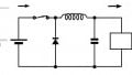
The push-pull topology is widely used for isolated DC/DC converters. It is a low-cost method of generating higher, lower, or inverted voltages since the transformer turns ratio determines the output voltage relationship. The topology is simple, reasonably efficient, and has relatively low electromagnetic emissions.

Figure 2. Push-pull DC/DC converter with unregulated output. Image used courtesy of Bodo’s Power Systems [PDF]
Figure 2 shows the block diagram of an isolated push-pull DC/DC converter with an unregulated output. To save space, the oscillator and drive transistors can be combined in a dedicated push-pull transformer driver IC.
For a regulated output, the simplest approach adds a linear regulator on the secondary side in series with the +Vout line, as shown in Figure 3. This approach achieves the desired goal and is suitable for the lowest wattage DC/DC designs. An example is the RECOM RY/P series, where the linear regulator offers short-circuit protection as well as a regulated, low-noise output.

Figure 3. Push-pull DC/DC converter with regulated output. Image used courtesy of Bodo’s Power Systems [PDF]
This type of design can achieve efficiencies of around 65–75%. Above 1 W or 2 W, maximizing efficiency becomes a higher priority, requiring further design refinement. Hence, instead of secondary-side regulation, primary-side regulation is used. In place of the linear regulator, the output voltage is monitored on the secondary side and compared to the desired voltage to generate an error voltage that is then sent back to the primary-side oscillator controller. This adjusts the switching frequency to drive the error toward zero. Since this is an isolated design, the error signal must be also isolated. Figure 4 shows this approach used in RECOM’s regulated converters rated 3 W and higher, allowing for efficiencies of around 85%.

Figure 4. Secondary-side error signal provides feedback to the primary-side controller. Image used courtesy of Bodo’s Power Systems [PDF]
A more sophisticated approach is needed for DC/DC converters with still higher power output. Not only does the linear regulator waste power in the manner discussed above, but the two secondary-side diodes are also sources of loss. A power diode has a forward voltage drop of typically 0.5V, which translates to a power loss of 0.5 W at 1 A.
The solution is to replace the diodes and linear regulator with a synchronous rectifier consisting of two FETs and a controller.

Figure 5. Passive rectification (left) vs. synchronous rectification (right). Image used courtesy of Bodo’s Power Systems [PDF]
Figure 5 contrasts the two approaches. The FETs act as rectifiers by switching on during the forward part of the cycle and turning off during the reverse part of the cycle. The combination of fast switching and very low on-resistance RDS(ON) of about 10 mΩ make FETs ideal rectifiers. The disadvantage is that they must be actively driven, so additional timing and drive circuits are required that sense the internal voltages and correctly turn on and off the two FETs synchronously with the output waveform. Diodes are passive devices that need no extra circuitry to function, but the increased efficiency afforded by synchronous rectification more than offsets the increased cost complexity for higher output current converters.

Figure 6. The RP20 incorporates numerous design techniques to boost efficiency. Image used courtesy of Bodo’s Power Systems [PDF]
The synchronous rectifier is used in RECOM’s RP20 family of 20 W DC/DC converters that can achieve efficiencies of up to 89%. This design also includes the isolated error signal described earlier. Lastly, the RP20 in Figure 6 can achieve efficiencies from 85–89% across a wide load range.
Design techniques borrowed from much larger power supply designs are being applied to the lowest-wattage DC/DC converters, yielding higher efficiencies. Since customer priorities change as power levels increase, appropriate modifications must be used. RECOM is a leader in picking the right designs for the best combination of cost and size.
This article originally appeared in Bodo’s Power Systems [PDF] magazine.