Facebook
 Google
 GitHub
 Linkedin
The PN Junction as a Rectifier
Learn about the traits of the rectifying p-n junctions in semiconductors.
The fundamental electrical characteristic of a P-N junction is that it facilitates the flow of charge in one direction while restraining the flow in the opposite direction, establishing a rectifying action. Initially, the vacuum tube diodes performed the rectification operations. But the P-N junctions replaced them.
The Crystal Radio
Natural semiconductors in the form of radio crystals or galenas have been known for many years. The crystal radio receivers were very popular in the early days of radio. The radio detector employed mainly galena, a crystalline mineral which is the natural form of lead sulfide – a non-metal. The detector converts the alternating current signal received in the antenna to direct current – a rectifying property – and demodulates an amplitude modulated signal. Now, a component with this property is called a diode.
Galena has a small energy gap – about 0.4 eV – between the valence band and the conduction band. Galena also has small quantities of impurities that will allow excited electrons to jump into the conduction band and conduct electricity. Galena radios do not need external power to accomplish this. The crystal radio impacted the worldwide expansion of wireless communications in the 20th Century.
The improved understanding of the conduction mechanism allowed replacing these primitive forms of rectification with today’s precisely optimized semiconductors.
This article will focus on p-n junctions as a primary example of the many semiconductor devices.
The P-N Rectifying Junction
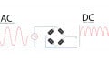
The P-N junction is a rectifier diode because it has asymmetric current/voltage characteristics, allowing the current to flow in only one direction. An example is the conversion of an alternating current into a direct current.
Figure 1 shows the I-V characteristic for a silicon P-N junction.

Figure 1. I-V characteristic for a silicon p-n junction.
The P-N Junction with Reverse Bias
Reverse bias occurs when connecting the negative terminal of a battery (DC) to the P-type side and the positive terminal to the N-type side of the P-N junction – making the N-type side more positive than the P-type side. Figure 2 shows the reaction of the charge carriers to the application of a reverse-biased potential.

Figure 2. Electron and hole distribution for reverse bias.
The connection polarity causes the holes in the P-type side and the electrons in the N-type side to move away from the junction, separating the positive and negative charges – polarization – and making a larger region around the junction free of mobile charge carriers.
The region of negative charge further spreads to the junction’s left, and the area of positive charge further expands to the junction’s right.
In reality, a small current flows due to the small quantity of hole-electron pairs generated throughout the crystal by thermal energy. The holes formed in the N-type side and the electrons created in the P-type side will wander over to the junction. This process generates the reverse saturation current (IS), which increases with temperature and is independent of the reverse bias’s magnitude. Consequently, the reverse resistance of the junction decreases with increasing temperature.
The reverse saturation current is in the order of a few µA and usually in nA, excluding high-power devices. It attains its maximum level quickly and does not change significantly with increases in the reverse-bias potential – this is why the term saturation is due.
Another way of explaining the mechanism of conduction in the reverse direction is considering the potential barrier across the junction with no voltage applied (V0) and the impact of using a reverse-biased potential V.
The N-type side will increase the number of uncovered positive ions in the depletion region due to the large number of free electrons drawn to the battery’s positive terminal. The P-type side will increase the number of uncovered negative ions in the depletion region due to the large number of holes drawn to the battery’s negative terminal. The result is the widening of the depletion region and a higher barrier for the majority carriers to overcome. The reverse bias potential adds to the barrier voltage, increasing the effective barrier voltage to V0+V.
The increased barrier’s height reduces the majority carriers’ flow, the number of holes diffusing into the n-type side, and the number of electrons diffusing into the P-type side. The additional barrier height does not influence the minority carriers’ flow – electrons in the P-type side and holes in the n-type side – since they fall down the hill.
To summarize, there is a considerable reduction of the diffusion current Id. A reverse bias voltage around one volt is sufficient to cancel Id. Then, the current through the junction and the external circuit will be the current Is. Recalling that this is the current due to the drift of the minority carriers – thermally generated – across the depletion region, IS will be very small and deeply dependent on temperature.
Figure 3 shows the rectifier (diode) symbol with the reverse saturation current’s direction, and the left-hand half of figure 1 shows the volt-ampere characteristic under the reverse-biased condition.

Figure 3. Reverse bias polarity and direction of Is.
The P-N Junction with Forward Bias
Forward bias occurs when connecting the positive terminal of a battery to the P-type side and the negative terminal to the N-type side of the P-N junction – making the P-type side more positive than the N-type side. Figure 4 shows the reaction of the charge carriers to the application of a forward-biased potential.

Figure 4. Electron and hole distribution for forward bias.
The battery’s positive terminal repels the holes while the negative terminal repels the electrons. Then, the majority carriers, electrons on the N-type side, and holes on the P-type side travel to the junction. As holes and electrons meet, they recombine, extinguishing one another. This process reduces the depletion region’s width, generating a majority carrier’s heavy flow across the junction.
The applied forward voltage V disturbs the equilibrium initially established between the forces tending to produce majority carriers’ diffusion and the restraining influence of the potential energy barrier at the junction. The forward voltage lowers the height of the potential barrier at the junction leading to a barrier voltage of V0−V across the depletion region.
The lower barrier voltage enables more holes to diffuse from the P-type side to the N-type side and more electrons to diffuse from the N-type side to the P-type side. The large number of charge carriers flowing across the semiconductor toward the junction produces a low resistance and an appreciable current. Hence, the diffusion current Id increases substantially.
The magnitude of the minority carrier flow – electrons from the p-type side to the n-type side and holes from the n-type side to the p-type side – does not change. Then, Id becomes many orders of magnitude larger than the reverse saturation current Is.
The current Id flows in the forward direction of the junction, as shown in figure 5.

Figure 5. Forward bias polarity and direction of Id.
Increasing the magnitude of the applied bias decreases the depletion region’s width. It rises the current exponentially – as shown in the right-half side of the volt-ampere characteristic in Figure 1.
The Junction Breakdown
An electric field of high magnitude applied across a dielectric material may abruptly excite large quantities of electrons to energies within the conduction band, resulting in a dramatic increase of the current through the dielectric. This phenomenon is sometimes accompanied by burning, localized melting, or vaporization, producing irreversible material degradation and failure. The dielectric strength or breakdown strength is the magnitude of the electric field that makes breakdown.
In a P-N junction, thermally generated carriers can support a small reverse saturation current, equal to Is. Assume that we apply a reverse current larger than Is. As before, the height of the potential barrier at the junction increases until Id = 0, and the only carriers crossing the junction are those thermally generated. But these carriers can support only the current Is.
As we increase the reverse voltage, the depletion region widens and we reach an adequately high junction voltage where a new mechanism enters to support the applied current. This new mechanism is the junction breakdown.
The high junction voltage is the breakdown voltage (VBR), or Zener voltage (Vz). At this reverse bias voltage, a vast reverse current flows, as shown in the left-hand half of figure 1 – a remarkable change in the volt-ampere characteristic.
Observe that the reverse voltage has a minimal increase while the reverse current rises noticeably – the reverse voltage across the junction stays very close to the value VZ.
The junction breakdown is not a destructive phenomenon as long as the junction has adequate power-dissipation capabilities to operate in the breakdown region. Hence, the p-n junction can frequently work in the breakdown region without impairing its characteristics. A practical application is an avalanche, breakdown, or Zener diode.
Two mechanisms for P-N junction breakdown are the Zener effect and the avalanche effect.
The Zener effect occurs when the electric forces created by the electric field in the depletion layer are enough to tear electrons out of the covalent bonds, making electron-hole pairs. The electric field drives the holes to the p-type side and the electrons into the n-type side, creating a reverse current across the junction.
The avalanche effect arises when the breakdown is at high voltage. The thermally generated minority carriers crossing the depletion region under the electric field’s influence collide with the crystal lattice members. With a high junction voltage, they gain sufficient kinetic energy to break covalent bonds in atoms with which they collide and create electron-hole pairs.
Again, the electric field drives the holes to the P-type side and the electrons into the N-type side. The movement of these carriers is equivalent to one carrier moving across the depletion region. They can have ionizing collisions, creating new electron-hole pairs in the fashion of an avalanche. The result is the formation of many carriers able to maintain any value of reverse current, with a tiny change in the voltage drop across the junction.
When a breakdown occurs with a voltage less than 5V in silicon, the mechanism is the Zener effect. Above 7V in silicon, avalanche breakdown is the mechanism. For voltages between 5V and 7V, the instrument might use either mechanism or a combination of the two.
The Rectification Process
Figure 1 shows that a P-N junction is a non-ohmic or nonlinear element. The cause of this behavior is the mechanism of charge motion across the component. A noticeable feature is that the junction’s volt-ampere characteristic is not symmetric. Then, reversing the voltage polarity does not generate the same current magnitude in the opposite direction.
Figure 6 exhibits the process of input voltage and output current when applying a sinusoidal and harmonic voltage of amplitude V0 to a nonlinear element with the volt-ampere characteristic curve shown. The result is a sinusoidal current that is not harmonic and varies between I1 and -I2. When the magnitude of I1 is much larger than the magnitude of I2, we have a rectification process.

Figure 6. A sinusoidal voltage applied to a nonlinear element.
If we apply a sinusoidal voltage to a P-N junction, the maximum of the current flow for the reverse bias voltage (Is) is extremely small compared to that for forward bias (Id). Then, the P-N junction acts as a rectifier, letting the current pass in one direction but not opposite.
About The P-N Rectifying Junction
A rectifier, or diode, is an electronic device that allows the current flow in only one direction.
A P-N Junction has the rectifier's properties.
The P-N junction exhibits unlike conduction properties in its reverse and forward directions.
The reverse-bias scheme connects a battery’s negative terminal to the junction’s p-type side and the positive terminal to the n-type side. In this manner, the voltage applied increases the contact potential difference and decreases the diffusion current considerably, while the drift current remains unchanged. A small reverse current results, and the depletion zone widens.
We deduce that with reverse bias, the current in the reverse direction – the reverse saturation current Is – is minimal and almost constant.
The forward-bias scheme connects a battery’s positive terminal to the junction’s p-type side and the negative terminal to the n-type side. In this way, the p-type side becomes more positive, and the n-type side becomes more negative, decreasing the potential barrier’s height. As a result, more majority carriers overcome this smaller barrier, increasing the diffusion current Id. The minority carriers sense no barrier, so there is no noticeable impact on the drift current.
Another result of forward bias is the narrowing of the depletion zone.
We conclude that the P-N junction can conduct a substantial current with forward bias – mostly a diffusion current.
High reverse bias voltages – sometimes of several hundred volts – generate large numbers of holes and electrons. This large amount of charge carriers increases the current abruptly, producing the material’s breakdown. Operation in this region causes permanent harm to the typical type of semiconductor diode and is therefore avoided. Certain diodes, like Zener diodes, operate, by design, in this region.
The resistance of a P-N junction changes with the applied potential difference and polarity. This feature allows the easy flow of current in only one direction, making the junction act as a rectifier.