Facebook
 Google
 GitHub
 Linkedin
Rectification Explained Part 2: Full-Wave Rectification
Rectification is a significant part of electric circuits, as it plays a role in converting AC voltage to DC voltage. This article will focus on full-wave rectification.
In Part 1 of the series, we introduced rectification and why it is necessary for electronics. Part 2 will focus on full-wave rectification.

Image used courtesy of Adobe Stock
Full-Wave Rectification
Full-wave rectification occurs in both negative and positive cycles. In other words, rectification is performed in a complete cycle. In modern electronics, two full-wave rectification configurations exist bridge full-wave rectifiers and center-tapped full-wave rectifiers. Both have their benefits and drawbacks.
Center-Tapped Rectifier

Figure 1. Center diagram of the center-tapped rectifier. Image courtesy of Simon Mugo
This type of full-wave rectification involves a center-tapped transformer secondary voltage whereby each coil end is connected to different diodes D1 and D2, and the center tapping is grounded.
The notable features of the center-tapped transformer used in this rectification are:
- The mid-point tapping voltage is zero and forms the neutral point.
- This tapping is carried out by connecting a lead in the center of the secondary winding of the transformer. The coil will, in this case, be split into two equal parts.
- This tapping separates output voltage into two equal amounts with different polarities.
- You can carry out several tappings, which offer different amounts of output voltages.
How Center-Tapped Full-Wave Rectification Works
By applying a positive half-cycle voltage to the transformer, point M of the transformer's secondary winding becomes positive. The action makes diode D1 forward-biased causing the current i1 to flow through point A to B, which is a path across the load resistance RL. The output results in a positive half-cycle. Figure 3 below is the circuit representation of this explanation.

Figure 2. The circuit indicating positive half-cycle current flow. Image courtesy of Simon Mugo
On applying a negative input on the secondary winding of the transformer half-cycle, point M concerning point N of the transformer’s secondary winding becomes negative. The diode D1 ends up being reverse-biased and D2 forward-biased. Forward-biasing diode D2 allows current i2 to flow through the load resistor Rl from point A to point B. This action results in a positive half-cycle at the output even when the input is a negative half-cycle.
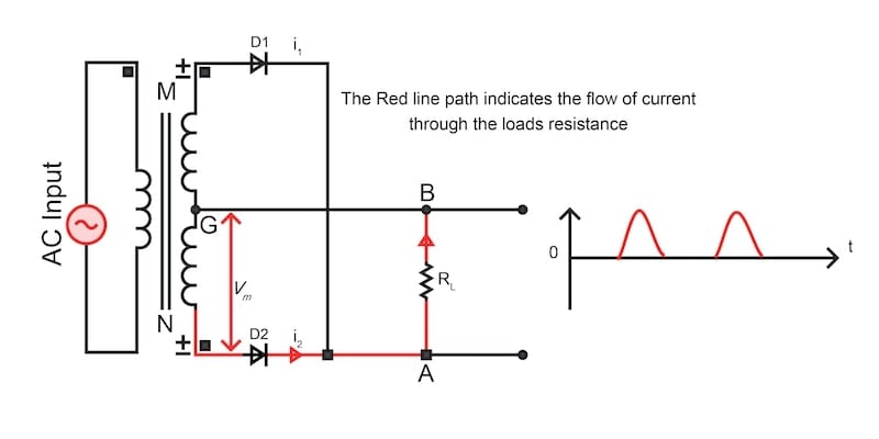
Figure 3. The circuit indicating negative half-cycle current flow. Image courtesy of Simon Mugo
Center-Tapped Full-wave Rectifier Waveforms
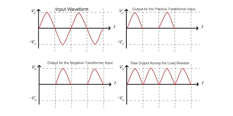
Figure 4. Center-tapped full-wave rectifier waveforms. Image courtesy of Simon Mugo
Figure 4 shows that output is derived from both the negative and positive half-cycles, and the output is the same direction for both the rectifier half-cycles.
Center-Tapped Full-Wave Peak Inverse Voltage
The maximum voltage across the transformer’s half-secondary copper windings is determined by Vm, and the whole of this secondary voltage appears at the nun-conducting diode. Therefore, the peak inverse voltage is double the maximum voltage across the transformer’s half-secondary winding.
The peak inverse voltage can be determined by:
\[PIV=2V_{m}\]
Disadvantages of the center-tapped full-wave rectifier include:
- difficulty locating the center tapping
- small output DC voltage
- PIV of the diode has to be very high
Bridge Rectifier
The circuit uses four diodes to not only produce a full-wave rectification but also address the disadvantages associated with the center-tapped configuration.
Diodes D1, D2, D3, and D4 are connected so only two diodes conduct at any given half of the cycle. There is no involvement of center tapping.

Figure 5. Circuit diagram of the bridge full-wave rectifier. Image courtesy of Simon Mugo
How Bridge Full-Wave Rectification Works
Inputting a positive half cycle to the bridge, point P goes positive as compared to point Q. This makes diode D1 and D3 forward biased while diode D2 and D4 remain reverse biased. Diodes D1 and D3 and the load resistor form a series connection and complete the conduction loop, shown in Figure 6. Now that two diodes work together to produce an output, the voltage produced will be twice that of a center-tapped full-wave rectifier.
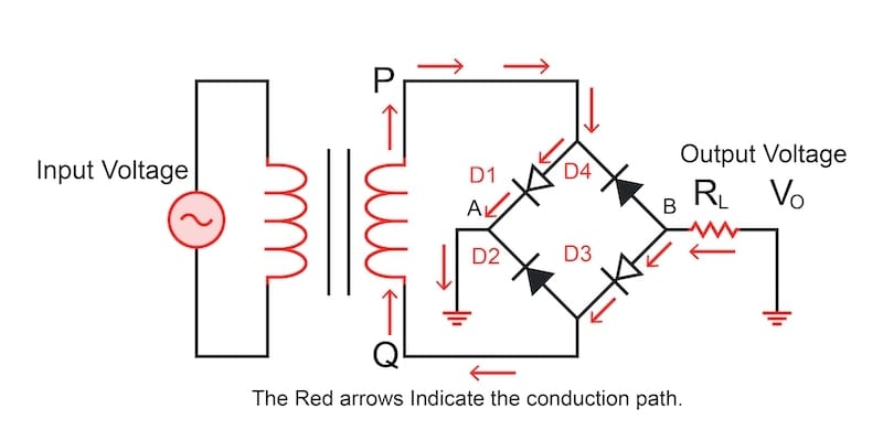
Figure 6. The positive input current flow indication circuit. Image courtesy of Simon Mugo
Injecting a negative half cycle at the input point of the circuit makes point P negative as compared to point Q, making diodes D1 and D3 reverse-biased while diodes D2 and D4 become forward-biased. The diodes D2 and D4 form a series loop load resistor and go to conduction mode, as shown in Figure 7.

Figure 7. The negative input current flow indication circuit. Image courtesy of Simon Mugo
The Waveforms of the Bridge FWR

Figure 8. The bridge full-wave rectifier waveforms. Image courtesy of Simon Mugo
Figure 8 shows the output obtained for both the negative and positive half-cycles, and both the half-cycle outputs have the same directions.
The bridge rectifier solves the disadvantages associated with the center-tapping rectifier.
Full-Wave Rectifier Analysis
For the analysis to be achievable, assume the input voltage Vi to be:
\[V_{i}=V_{m}sin\omega t\]
The current in the RL or diode is determined by the equation:
\[i_{1}=I_{m}sin\omega t\,\,\,for\,0\leq\omega t\leq\pi\]
\[i_{1}=0\,\,\,for\,\pi\leq\omega t\leq2\pi\]
Where
\[I_{m}=\frac{V_{m}}{R_{f}+R_{L}}\]
Similarly, the current in the RL or diode is determined by:
\[i_{2}=0\,\,\,for\,0\leq\omega t\leq\pi\]
\[i_{2}=I_{m}sin\omega t\,\,\,for\,\pi\leq\omega t\leq2\pi\]
The total current through the load resistance is the sum of all the currents:
\[i=i_{1}+i_{2}\]
Average or DC Current
The average current output can be derived as:
\[I_{DC}=\frac{1}{2\pi}\smallint^{\pi}_{0}i_{1}d(\omega t)+\frac{1}{2\pi}\smallint^{2\pi}_{0}i_{2}d(\omega t)\]
Replacing the equations of i1 and i2 and completing the integration we find that
\[I_{DC}=\frac{2I_{m}}{\pi}=0.636I_{m}\]
Comparing this with what we got while analyzing the half-wave rectifier, the value is double.
Output DC Voltage
The output DC voltage of the full-wave rectifier is determined by the equation:
\[V_{DC}=I_{DC}R_{L}=\frac{2I_{m}R_{L}}{\pi}=0.636I_{m}R_{L}\]
The value is twice the half-wave rectifier’s DC voltage output.
The RMS Current
The equation for the RMS current can be derived as:
\[I_{RMS}=\sqrt{\frac{1}{\pi}\smallint^{\pi}_{0}sin^{2}\omega t\,d(\omega t)}\]
With two currents of the two halves, which are equal in both halves, the equation becomes:
\[I_{RMS}=\sqrt{\frac{I_{m}^{\,\,\,\,\,2}}{\pi}\smallint^{\pi}_{0}sin^{2}\omega t\,d(\omega t)}\]
\[I_{RMS}=\frac{I_{m}}{\sqrt2}\]
Efficiency of the Rectifier
\[\eta=\frac{Output\,DC\,Power\,of\,the\,Load}{Input\,AC\,Power\,from\,the\,Transformer}=\frac{P_{DC}}{P_{AC}}\]
\[P_{DC}=(\frac{V_{m}}{\pi})^{2}\]
\[P_{AC}=(\frac{V_{m}}{\sqrt2})^{2}\]
Replacing the above in the efficiency equation, the efficiency becomes:
\[\eta=\frac{8}{\pi^{2}}=0.812=81.2\%\]
Ripple Factor
The form factor is calculated as follows:
\[F=\frac{I_{RMS}}{I_{DC}}\]
Replacing current values in the formula you get that the form factor is 1.11
The ripple factor is now given by;
\[\gamma=\sqrt{F^{2}-1}\]
Replacing the right values, ripple factor is 0.48.