Facebook
 Google
 GitHub
 Linkedin
Implementing Hybrid ANPC Inverters With Synchronous Rectification
Manufacturers of PV inverters and energy storage systems are increasingly turning to silicon carbide power modules to increase the efficiency of their solutions. This article discusses how to implement hybrid active neutral point clamped (ANPC) inverter topology with synchronous rectification to balance efficiency and cost for common applications.
This article is published by EE Power as part of an exclusive digital content partnership with Bodo’s Power Systems.
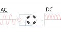
PV installations with battery storage are gaining popularity, driven by the need for a more resilient energy infrastructure to supply demand fluctuations. Unlike conventional solar inverters, which only need to support a power factor range from 0.8 to 1, bi-directional inverters supporting battery charging from the power grid also need to operate at a power factor of -1. The advantages of the active neutral point clamped (ANPC) inverter topology for such bi-directional operation are well established, and leading PV inverter manufacturers have already adapted it into their solutions.

Image used courtesy of Adobe Stock
With the rising price per kWh, equipment manufacturers are looking to further increase the efficiency of their solutions while minimizing the required system-level modifications to their designs. To do so, they are turning to silicon carbide components to leverage their higher power density and reduced ohmic losses compared to standard silicon components.

Figure 1. Until the cross-over point of the I-V characteristic of the diode and the MOSFET channel, synchronous rectification offers significant conduction loss savings. Image used courtesy of Bodo’s Power Systems [PDF]

Figure 2. Comparing the outer switch modulation and inner switch modulation in terms of topology (left and right) and cost (middle). Image used courtesy of Bodo’s Power Systems [PDF]
In this article, we lay out how to optimize the power efficiency and cost of the ANPC inverter topology using synchronous rectification (SR). We provide insights into selecting the optimal ANPC topology to fully take advantage of the capabilities of increasingly popular SiC MOSFETs. Finally, we present simulations comparing module losses and efficiency with alternative approaches.
What Is Synchronous Rectification?
But first, what is synchronous rectification, and what role does it play in increasing the efficiency of current rectification? Synchronous rectification is a method that reduces conduction losses in the freewheeling path by replacing the diode PN-junction voltage drop with the resistive channel of a MOSFET.
Figure 1 presents the conduction loss of a diode as well as that of a MOSFET channel at 25 °C and 125 °C. The conduction loss savings are given by the area between the curves indicated by the red arrow. Up to the cross-over point of both I-V characteristics, synchronous rectification offers significant conduction loss savings.
Note the temperature dependence of the cross-over point: While the forward voltage over the diode decreases with rising temperature, the MOSFET’s resistance in the on state, Rds(on), increases, with the cross-over point moving in favor of the diode.
ANPC at a Glance
The active neutral point clamped inverter topology converts a DClink voltage to an alternating voltage with variable frequency. In contrast to a half-bridge or six-pack, the ANPC topology offers an additional voltage level at the output, which can not only jump to DC+ and DC- but also to zero. It is primarily used in high-efficiency three-phase PV inverters and applications with bi-directional operation requirements, such as battery storage. In most standard applications, the blocking voltage of the components is 950 V or 1200 V, enabling DC-Link voltages beyond 1500 V. This makes ANPC inverters a perfect match for 1500 V applications.
The three-level ANPC topology, which features six active switches (IGBTs or MOSFETs) and four to six diodes, typically uses one of two main modulation techniques: outer and inner switch modulation. In the case of outer switch modulation, the four switches connected to the DC link are switched with the desired choke frequency (typically > 16 kHz), while the other two switch at line frequency (50- 60 Hz). The situation is inverted in inner switch modulation, where the four switches connected to the DC link are switched at line frequency and the other two at the desired choke frequency.
While both schemes are on par in terms of power efficiency, they differ in terms of other critical factors, namely simplicity and cost. Because only SiC MOSFETs deliver the switching speeds required for the high-frequency switches, outer switch modulation requires them in four positions, significantly increasing the cost compared to inner switch modulation, which only needs two. Moreover, implementing synchronous rectification for outer switch modulation, which uses different switching pairs for the positive and negative sine cycles, requires a much more complex pulse width modulation (PWM) scheme.
Meanwhile, inner switch modulation uses the same switching pairs for all operation modes. Implemented as a hybrid circuit using four silicon insulated-gate bipolar transistors (IGBTs) and SiC MOSFETs in two positions, inner switch modulation is the most cost-effective solution, offering the best topology for applications using SiC MOSFETs and synchronous rectification.
ANPC With Inner Switch Modulation
The optimal implementation of the ANPC topology with inner switch modulation depends on the specific design constraints of the end application. The figure below represents two variations of the topology. The first uses the MOSFET’s conducting channel as the freewheeling diode, which, as we’ve seen, is the basis of synchronous rectification. The second decouples the high and low side switches and adds an additional freewheeling SiC Schottky barrier diode (SBD) in parallel to the MOSFET body diode.

Figure 3. Comparing inner switch modulation with synchronous rectification (left) with the use of additional freewheeling SiC SBDs in parallel to the MOSFET body diode (right). Image used courtesy of Bodo’s Power Systems [PDF]
Cost-sensitive applications typically prefer the first variant, which uses fewer components and offers the lowest module cost due to minimized SiC content. Note that synchronous rectification is mandatory here due to the high forward voltage of the MOSFET body diode. An example of this topology is the LR88 family of Vincotech ANPC inverter modules.
Applications with SiC MOSFETs that are sensitive to re-turn on are, on the other hand, better served with the second variant, which uses freewheeling SiC SBDs, but at a higher module cost due to the additional SiC components. While synchronous rectification is not required using this topology, it can be used to further increase efficiency. An example of this topology is given by the LC59/69 family of Vincotech ANPC inverter modules.
The PWM Pattern for ANPC With Synchronous Rectification
When implementing the ANPC with synchronous rectification, the basic PWM pattern and duty cycle definition correspond to that of a conventional ANPC. The difference is the separation of the freewheeling time into three phases. The following section shows the freewheeling phases using the example of a positive line voltage and current.
| time | T13 gate | T14 gate | Comment |
| t0 | on | off | Excitation, inductor current increasing |
| t1 | off | off | Freewheeling through T14 body diode |
| t2 | off | on | Freewheeling through T14 channel |
| t3 | off | off | Freewheeling through T14 body diode |
| t4=t0 | on | on |

Figure 4. The PWM pattern for ANPC with synchronous rectification. Image used courtesy of Bodo’s Power Systems [PDF]
t1-t2: The current flows through the MOSFET body diode (T14).
This phase ensures proper commutation and avoids cross-conduction during the turn-off of T13 and the turn-on of T14. With perfect drive signal matching, this time could theoretically be optimized to zero.
t2-t3: The MOSFET is turned on, and current flows through the conducting channel. This phase should be made as long as possible to maximize efficiency gains.
t3-t4: The MOSFET is turned off, and current flows through the body diode. This last phase ensures proper commutation and avoids cross-conduction during the turn-off of T14 and the turn-on of T13. With perfect drive signal matching, this time could theoretically be optimized to zero.
Comparing Efficiency
To compare the efficiency of ANPC with synchronous rectification with an implementation using a body diode and another one using a SiC SBD, we first determined the boundary conditions for our simulation.
For this, we evaluated the typical I-V characteristic of a SiC MOSFET using the Vincotech flowANPC S3 power module using inner switch modulation without a freewheeling diode in parallel to the SiC MOSFET body diode.

Figure 5. The typical I-V characteristic of a SiC MOSFET at a junction temperature, Tj, of 150 °C. Image used courtesy of Bodo’s Power Systems [PDF]
Synchronous rectification takes place in the third quadrant (Q3). During this phase, the MOSFET channel is fully conducting, with a gate-to-source voltage (VGS) higher than 14 V. The MOSFET channel voltage drop is lower than that of its body diode.

Figure 6. Comparing the efficiency in terms of power and cost of ANPC with (i) SR, (ii) the MOSFET’s body diode and (iii) an additional SiC SBD. Simulation conditions: Vdc=1350V, Vac=460V, cosphi=0.8, fsw=16kHz, Rg=4R, Ths=80°C. Image used courtesy of Bodo’s Power Systems [PDF]
At a junction temperature, Tj, of 150 °C and a current of -250 A, the MOSFET channel voltage drop, VDS(SR), is -2.5 V, while the body diode voltage drop is - 5 V.
Comparing the efficiency of ANPC with synchronous rectification with an implementation using a body diode and another using a SiC SBD, shown in Figure 5, revealed that ANPC with synchronous rectification offers the highest efficiency over the entire power range. It also showed that ANPC benefits the most from synchronous rectification at high output power, leading to fewer losses and higher efficiency. At lower output power, the advantages of synchronous rectification are less due to the low freewheeling current.
As can be seen in the figure, additional SiC SBDs for freewheeling almost match the efficiency of SR but at a cost increase of 18% to the module. And as anticipated, due to the high forward voltage, using the SiC MOSFET’s body diode is a poor choice for freewheeling at high currents.
Boosting the Efficiency of Your Power Application
In this article, we presented the optimal ANPC inverter topology for emerging applications, such as PV inverters and battery storage solutions. In particular, we saw that ANPC with inner switch modulation is more cost-effective than the topology with outer switch modulation due to its lower SiC content.
Doing away with the SiC SBD freewheeling diode and using the SiC MOSFET reverse conducting channel brings additional benefits. These include reducing the number of required components, freeing up space on the DCB, and further reducing module cost with no loss of performance. In fact, ANPC with synchronous rectification offers higher efficiency than ANPC with SiC SBDs and, in most cases, requires no changes to the system architecture, including the gate drive circuits and even the microcontroller.
Finally, ANPC with synchronous rectification, as delivered by the Vincotech flowANPC S3 power module, ranks first in terms of its price-performance ratio, making it an ideal solution for wide-ranging power electronics applications. Learn more about the APNC inverter topology at vincotech.com and explore our full range of inverter modules tailored to the needs of PV, battery storage, and uninterruptible power supplies (UPS) applications.
This article originally appeared in Bodo’s Power Systems [PDF] magazine.