Facebook
 Google
 GitHub
 Linkedin
The Power of Diamond as a Semiconductor
Could diamond be the ultimate semiconductor for power electronics?
This article is published by EEPower as part of an exclusive digital content partnership with Bodo’s Power Systems.
In a global economy yearning for technology as a solution to climate change, power electronics are one of the keys to the electrification and decarbonization of society. AI and data centers, mobility electrification, industrial electrification, renewable energy integration, energy storage, and green hydrogen production need suitable power electronics. Each application has its own technical, environmental, and economic constraints.
What are the challenges in power electronics? One can argue that power electronics are a tradeoff at the component and system levels. In an ideal world, every application would require power electronics without power losses, with a minimum size (volume and weight), and at low costs. The dilemma in power electronics is that customers cannot have it all, which is physics' fault.
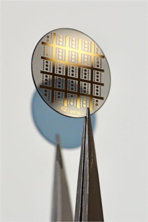
Image used courtesy of Bodo’s Power Systems [PDF]
Tradeoffs
Due to the physical properties of the semiconductor used in the components, there will always be losses during power conduction and switching, and there will always be passive and cooling systems to extract the heat from losses, which comes at a cost. Therefore, there will always be a choice to find a good tradeoff for every application.
For example, if priority is given to efficiency, this will impact bigger sizes and lead to higher costs. Let’s assume the solution is to increase the voltage level of the system. As U = RI and power losses are P=RI2, if we double the voltage, we cut the current by a factor of 2, and losses are reduced by a factor of 4. However, by doing that, the components must adapt to the new voltage level. The RDS(on) of the component follows (very approximately) the square curve with the voltage, so to keep the same resistance at doubled voltage, the component's surface required will also be increased by a factor of 4. By doing that, the costs will be significantly higher than the previous components. But it is still not finished!
By increasing the surface, the switching losses will also be increased. A deep study to find the best tradeoff needs to be done. A deep study to find the best tradeoff needs to be done. Moreover, this example only assumes one possible solution; there are many others, but they come with drawbacks. Other factors, such as junction temperature, can also impact the efficiency.
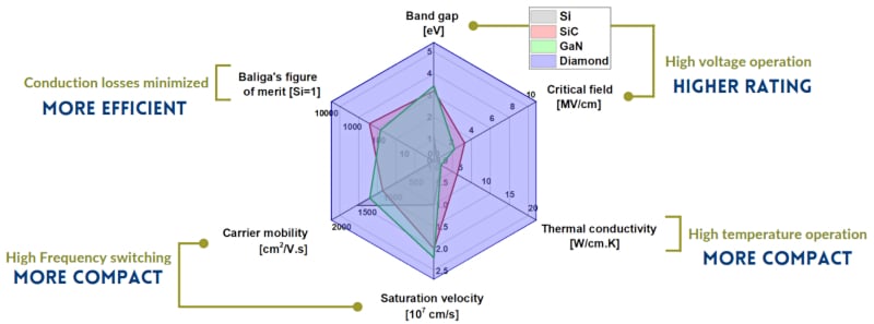
Figure 1. Image used courtesy of Bodo’s Power Systems [PDF]
When turned on, the resistance of the component and the current going through generate joules losses. In most semiconductors, dissipating the heat and keeping the power semiconductor cooled (or as close to room temperature as possible) will prevent designers from overrating components and allow an overall higher efficiency. The cooling system required can be bulky, costly, or both.
The same goes for size and volume reduction or power density increase. The main drivers for reaching such goals are increasing switching frequencies (to reduce the size of passive components) and implementing active cooling systems to reduce their size compared to a passive cooling system. The first action increases the energy losses, the second increases the costs. There is always a drawback.
Diamond semiconductor has the properties to make the tradeoff decisions much easier.
The main properties to be highlighted are ultra-wide band gap (5,5 eV), exceptional carrier mobility (2000 & 1000 cm2 v−1 s−1 respectively for holes and electrons), breakdown voltage (10 MV/cm), best-known heat conductivity (22 W cm-1 K-1). These properties allow for increased voltage of the components, increased efficiency, and reduced losses and costs. It means that to reach a certain performance (let’s say 1 mΩ @1000 V transistor), the diamond will need much less surface area of material and less active thickness than current commonly used semiconductors.
As an example, imagine you have a diamond component of the surface equivalent of a basketball ball with a given resistance for a 1000 V breaking voltage capacity. The equivalent surface of silicon required to reach the same resistance for the same voltage rating would be a complete basketball field.
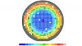
An interesting characteristic of diamonds is the resistance variation with temperature. Due to incomplete ionization at room temperature, the resistivity has a negative coefficient with temperature. It means that a diamond power transistor will perform better at 200°C (or even at 300°C) than at room temperature. This characteristic opens up two questions. First, the parallelization of components needs to consider this characteristic. The risk is that as the temperature rises on the component with lower resistance, the difference between the other parallel components increases, and eventually, all the current goes through to the same component, causing damage. Thanks to the exceptional thermal conductivity, the temperature difference inside the die is less than 0.1 °C.
More importantly, the cooling system does not need to be as big as possible; it should be dimensioned enough to keep the junction temperature at the suited high temperature. This is a game changer because to improve global efficiency, there is management needs to be done in heat extraction. In terms of thermal management, diamond enables a system where the efficiency peak is reached at a high temperature, and the junction temperature can be as high as the packaging limitation. The cooling requirements are, therefore, drastically reduced.
Diamond semiconductors will also open up new possibilities for engineers when designing the system. Depending on the main target of the engineer (system cost vs efficiency vs volume), diamond components will be able to adjust to the needs. For example, if the main goal is to reduce costs, diamond components will allow an increase in switching frequency compared to the current and, therefore, decrease the passive component's costs, also reducing the component costs.
Finally, diamond technology decreases CO2 emissions, not only during utilization but also during the manufacturing steps. Compared to other semiconductor technologies that need very high temperatures (> 2000°C), diamond manufacturing requires electricity to create ideal plasma and pressure conditions for epitaxial growth. Unlike other semiconductor materials, there is no utilization of SF6 during the etching process, which is a major greenhouse gas. H2 and CH4 are the two main components required as raw materials, and both can be obtained with a very low level of carbon emissions: hydrogen can be produced from renewable energy (green hydrogen), and methane can also be obtained from biomass. We estimate that there is at least a factor of 10 in CO2 reduction compared to silicon carbide.
At a glance, a system-level diamond brings value to all key parameters for better power efficiency on three major elements:
- Thermal management simplification/reduction
- Better tradeoff between component & system competitiveness/ energy efficiency and volume and weight reduction
- Reduced CO2 emissions for producing diamond wafers compared to other semiconducting materials
In terms of technology development, there are three historical roadblocks that need to be solved before expecting diamond to become a commercial reality: diamond wafer size, diamond wafer quality (in terms of dislocation and killer defects), and diamond doping.
Developments in the Diamond Industry
Diamfab's development efforts focus on quality (default density reduction) and doping mastering. Growing big enough diamond crystals is not an easy task. However, while for other semiconductor technologies, R&D investment has come from defense applications, the diamond industry is also leveraging knowledge from other industries, such as jewelry. The evolution is accelerating quickly. Four-inch single crystal wafers (100 mm) have already been demonstrated, whereas only 3 mm wafers were available a few years ago.
Diamond is different from most semiconductors in terms of the doping process. Diffusion or implantation processes are not suitable or recommended. The carbon lattice of diamond is so dense that dopant atoms such as boron, nitrogen, or phosphorus do not penetrate by diffusion technique. On the contrary, dopant atoms damage the carbon lattice, making diamonds non-usable for power electronics. Therefore, diamond doping is done “in situ,” which means that the dopants are included while the carbon atoms are on the way to being organized as diamond. Diamfab masters the manufacturing doping process, from non-intentionally doped to the metallic transition (highly doped), with high homogeneity in the x,y, and z-axis. Finally, crystal quality is also a topic that Diamfab is currently working on, and we hope to announce good news about this topic soon.
In a nutshell, the main technological bricks are solved, or there is a clear view of how to solve them, both from the material and the component manufacturing side. We have also learned a lot from the developments performed in compound semiconductors.
Diamond as a semiconductor will be an alternative product this decade. Diamfab has already achieved components with breakdown voltage above 1000 V (on just 1.7 µm of diamond thickness) reaching current densities > 1000 A/cm2 and transistors with a breakdown voltage above 3.5 kV have been demonstrated, too. Finally, we invite power electronics players working with other semiconductors, from academia to integrators, to explore diamond potential and learn how they can apply their expertise to this technology that is about to come. There are many topics to develop with a promising future ahead.
This article originally appeared in Bodo’s Power Systems [PDF] magazine and is co-authored by Gauthier Chicot, CEO, and Ivan Llaurado, CRO and Director of Partnerships, Diamfab.
.