Facebook
 Google
 GitHub
 Linkedin
Side Wall Gate - Moving on from Trench
This article discusses the new side wall gate structure and its performance characteristics and its module-level investigation.
A new Side Wall Gate Structure Shows Inspiring Performance Characteristics, Breaking Through the Trench Gate Ceiling. HITACHI Bridges the Performance Gap Between Silicon and Wide Band Gap Devices.
It is not news that the IGBT remains the backbone of the majority of inverter designs. Its bipolar structure enables handling of large powers and brings with it opportunities to improve efficiency targets of industrial, traction, T&D and automotive applications alike. Wide Band Gap devices, benefitting from a unipolar structure and all but eliminating recovery losses, dominate recent news. Hitachi is a firm advocate of this exciting technology, publishing academic papers and launching several new SiC high voltage products in the nHPD2 package. However, this does not necessarily mean that Silicon-based technologies do not have a market.
Introduction
Dominating the power semiconductor market since its introduction, the IGBT has delivered evolutionary performance improvements but there has perhaps been little revolutionary progress. In the 1980s Planar gate IGBTs were the sole core silicon process technology, before the availability of Trench gate designs in the 1990s. Since this step change, Trench gate has fast been approaching performance saturation. SiC is positioned to take up the needs for continuous improvement, although not without its own challenges. Cost versus reliability is one simple example. Endeavouring to bridge the gap between Trench gate and SiC MOS designs, whilst conscious of both two key market forces, cost and reliability, HITACHI positions itself to launches first products based on a revolutionary technology: Side-Wall Gate (SWG).

Figure 1: Schematic cross-section of IGBT unit cell structure
Fundamental structure
The Side Wall Gate IGBT adopts a new structure of IGBT in which a thick oxide layer covers the majority of the gate surface, exposing less area to the floating p well and n- doped channel regions. This structure has a direct positive influence on reducing the Miller capacitance (Cres) which subsequently results in the trade-off relationship improvement between the diode reverse recovery (dv/dt) and combined turn_on and diode turn_off switching losses (Eon+Err), when compared to conventional IGBT structures. At the same time, the decreased Cres shows IGBT turn_off loss reductions.

Figure 2*: Side Wall Gate vs. Trench: Cres / Vce dependence

Figure 3*: Diode recovery dv/dt vs. (Eon+Err) trade-off (1700V IGBT)
Motivations
Whilst semiconductor device manufacturers can target and realise very fast switching solutions to reduce the system costs of expensive, large and heavy wound components in particular, not all applications are able to extract all that the datasheet promises to offer. For instance, in motor control, restrictions will be imposed by the motor insulation specification, which will likely force the inverter designer to reign in their ambitions to switch faster as dV/dt levels reach or surpass the motor’s safe operating conditions. If forced to limit switching speed because of dV/dt limits, the performance benefit of a wide bandgap module, for example MOS SiC, may be lost and the cost will abruptly become a critical gateway. In such instances, a bridging solution becomes of greater interest and a key motivation for HITACHI developing the Side Wall Gate device structure.
Let us consider 600V-1200V devices adopted in an inverter design. Switching frequency (fsw) is assumed to be relatively high, particularly if we benchmark against 6500V applications: kHz switching rather than Hz. As such, the reduction of switching losses will be most important due to the dominance of switching events versus static conduction. It is also vital to suppress the surge voltage during switching to provide a rugged system design with high reliability.
Now consider the Automotive sector, one market sector quickly adopting IGBT technology for traction drive, compelled to improve CO2 emissions by EU6c standards. Several mandatory constraints are placed upon the OEMs: cost; size; reliability. Despite these, the driving experience must still deliver superior performance. WBG devices would be a logical starting basis for the drive inverter, but system costs may climb if switching frequency is limited to 12kHz by the electric motor. The challenge. To achieve improved switching loss characteristics without breaching the motor insulation limits. Considering this, the Side Wall Gate IGBT structure shows suitable promise, especially when battling the cost-performance quid pro quo. In a highly competitive price environment, high voltage SiC devices can sometimes be a victim of their own success, falling foul of commercial system demands, despite their inherent technical advantages. On the other hand, based on a Silicon bulk wafer and existing manufacturing lines, Side Wall Gate aligns closely with traditional Planar and Trench manufacturing costs, supply chains and lead-times.
Side Wall Gate: Automotive 1200V IGBT
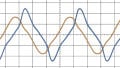
Figure 4 shows indicative simulation results of turn_off waveforms between a recent conventional Trench gate and the new Side Wall Gate (SWG).
SWG allows >30% faster turn_off, which is derived from the smaller Miller capacitance. On the other hand and importantly, despite the faster IGBT turn_off, the di/dt at which the peak voltage is reached shows the same level as the conventional device structure. Thus, the peak voltage is also the same level. Turn_off loss (Eoff) is in the region of 40% lower compared to the conventional Trench IGBT under same VCE(sat) as shown in Figure 4.

Figure 4: Simulated turn_off comparison
The turn_on waveform comparisons are given in Figure 5. SWG shows faster turn_on characteristics, in a similar manner to the turn_ off. The peak current of SWG is even smaller than the conventional IGBT. Both the SWG IGBT and diode characteristic improvement enable this desirable characteristic – Eon reduction 12%.

Figure 5: Simulated turn_on comparison
The counter arm diode reverse recovery is shown in Figure 6. Both peak current and tail current are smaller using SWG technology, culminating in a 9% improvement to the diode reverse recovery loss (Err). A reduction despite the diode VF being the same for both devices.

Figure 6: Simulated diode turn_off comparison
Module level investigation
In order to confirm the device level characteristics against the simulation data, SWG IGBTs were assembled into the HITACHI 98.5mm x 168mm pin-fin platform package shown in Figure 7. Results concur with the simulation modelling and measurement waveforms of IGBT turn_off, turn_on and diode reverse recovery are shown in Figure 8 respectively.

Figure 7: 400A/1200V 6-in-1 Test sample
Eoff of the new Side Wall Gate IGBT confirms a smaller power less than that of the conventional IGBT. Similarly, Eon+Err is in line with the simulation data where a suitable Rg is applied.
Owing to the smaller Miller capacitance of the SWG design, the gate-emitter voltage becomes more stable with a lower Vge peak. This distinguishing feature, compared to a conventional Trench gate design, generates a 30% lower short circuit peak current.

Figure 8a: Measured turn_on

Figure 8b: Measured turn_off

Figure 8c: Measured reverse recovery
Next steps
Following the first Side Wall Gate MBB400TX12A product release in Q4/2017 (3-phase pin-fin module rated 400A/1200V), the line-up will be expanded to reach the 6500V voltage class. Covering 600V to 6500V will bring the significant merits of Side Wall Gate, the first Silicon-based technology leap for 20 years, to all traditional applications of module-based IGBTs. Package platforms in pin-fin supported by future releases in both traditional HV-IHM and the new standard package platform nHPD2. MBN1000FH65G2 will be the flag-ship Side Wall Gate product rated 1000A 6500V and available for sampling.
Supplementing the first Side Wall Gate “A” series specifications for 600-1200V and “G2” series high voltage line-up (>1700V), follow on development activity has been presented on the academic circuit. Y. Takeuchi “A Novel Hybrid Power Module with Dual Side Gate HiGT and SiC-SBD” ISPSD 2017, shows the long-term future promise Side Wall Gate technology has to offer.

Figure 9: Type I short circuit waveform (VGE, 15V)
Conclusion
HITACHI has concluded the first phase of its strategy to bridge the large gap between the Silicon and Silicon Carbide cost-performance trade-off. Realising a low Cres cell structure, Side Wall Gate, enables higher frequency switching with 20% lower losses but avoiding increased stress to motor insulation. Based on traditional Silicon raw material, reliability is a known quantity and cost-effective, particularly for larger volume applications including the Automotive traction powertrain against the higher performing but higher cost wide band gap devices.
About the Author
Neil Markham works as the Product Marketing Manager of Power Devices Division at Hitachi Europe Lt., a European branch of the highly diversified Japanese company, Hitachi Ltd., that operates eleven business segments: Information & Telecommunication Systems, Social Infrastructure, High Functional Materials & Components, Financial Services, Power Systems, Electronic Systems & Equipment, Automotive Systems, Railway & Urban Systems, Digital Media & Consumer Products, Construction Machinery and Other Components & Systems.
This article originally appeared in the Bodo’s Power Systems magazine.