Facebook
 Google
 GitHub
 Linkedin
Scalability of SiC Near Chip-Scale Packages for Electric Vehicle & Locomotive Traction
This article introduces the µMaxPak, a proprietary power QFN package using automated low-cost QFN assembly technology.
µMaxPak packaging enables full SiC performance, efficiency & speed at high currents & voltages for traction applications
Power WBG/SiC devices traditionally packaged in bulky DBC modules can be replaced with Near Chip-Scale SMD packages. The replacement is enabled by the WBG device’s smaller die size (higher power density) and its higher efficiency. Near Chip-Scale packages like the µMaxPak can reduce package sizes & parasitics, enabling SiC devices to operate at their full performance, efficiency & speed.
These devices further enable higher density planar systems with enhanced system performance & efficiency. Power µMaxPak devices can be fully pre-tested before system assembly, reducing compound yield losses and assembly costs. The µMaxPak is a proprietary power QFN package, using automated low-cost QFN assembly technology, increasing throughput, and further reducing manufacturing cost. The requirements for µMaxPak type packages are explained in my July 2018 Bodo’s Power Systems article, “Inevitability of Near Chip Scale SMD Packaging for Power GaN & SiC.”
SiC switches in µMaxPak Near ChipScale packages can power heavy-industrial equipment, and EV and locomotive traction. µMaxPak switches are described below with cross-sections of examples in Figures 1, 2 & 3. The higher power products are very thin, so thicknesses are not to scale and have been exaggerated to show key structural features.
First Focus was on Light-Industrial Power Switches
The µMaxPak initial focus was up to 650V/400A & 1200V/200A industrial switches. Maximum die size was limited for solderability directly to power PCBs, DBC substrates, or even heavy copper lead frames, thereby limiting the maximum current. Initial µMaxPak designs, Types

Figure 1: Light-Industrial SiC 600-1200V µMaxPak Cross-Sections
Top/left: high-side switch Top/right: low-side switch
Bottom: half-bridge switches
I and II, brought all thermal & electrical connections from the top & bottom of the SiC die to the bottom of the SMD packages. They accommodated both lateral GaN and vertical SiC die. Near Chip-Scale SMDs are a significantly advanced alternative to DBC Modules used to package 600-1200V IGBT switches. These modules were bulky, slow & expensive, and although their huge parasitics were acceptable for silicon power devices, they greatly limit the performance of power WBG (GaN & SiC) devices. Figure 1 shows the basic structure of the Industrial µMaxPak a) high-side, b) low-side & c) half-bridge switches.
For Type I & II µMaxPak SMD packages, the pad area on the package bottom limits the available space and maximum current, and the available pad spacing limits the maximum voltage. As the new Type III µMaxPak’s with top & bottom pads evolve, they can be used to extend the current range for industrial 600V-1200V products. It is advantageous for light-industrial µMaxPak to have all bottom-side pads for standard SMD assembly processes.
Scalability to Electric Vehicle (EV) Traction Higher Currents: Type III or Thin µMaxPaks eliminate the over-molding on the top-side of the package, enabling electrical & thermal pads on both the bottom and topsides, which can accommodate higher currents like 750A & higher. The molding operation is essentially a filling of open spaces in the double-sided etched leadframe. This molding operation requires the leadframe & mold to be designed for molding compound fill & flow. The double-sided pads of the Type III µMaxPak also require both sides to be deflashed & plated.
Type III µMaxPak packages require vertical WBG die like the SiC MOSFET with drain (D) on one side and source/gate (S/G) on the opposite sides. (Today’s lateral GaN on SiC substrates can be used if the D is brought to the back/opposite side of the die with via.) Larger top & bottom pads accommodate higher current for 600V-1200V EV Traction switches. Figure 2 shows the basic structure of the EV µMaxPak a) high-side (HS) & b) low-side (LS) switches.
The higher EV currents increase the required die size, necessitating the µMaxPak can be soldered only to DBC substrate isolators to minimize the CTE expansion mismatch to the exposed bottom-side die. These substrates must provide the lowest thermal resistance with high-voltage isolation.

Figure 2: EV Traction 650-1200V SiC µMaxPak Cross-Sections
Top: high-side switch Bottom: low-side switch
The top of HS & LS µMaxPak switches will be soldered to an output bus, which again has CTE mismatch issues between the exposed SiC die and the copper output bus. Therefore, the high current contacts require multiple pads with stress relief features between the pads. Stress relief can be achieved with multiple thin and narrow connectors, and C-bends.
A secondary forming or coining operation to the etched leadframe strips can create both stress-relief & HV clearance features. This operation enables the one-piece power QFN leadframe, which is a key feature of the µMaxPak cavity architecture described in U. S. patent 9,214,416.
Higher power Near Chip-Scale packages with power-pads on both top & bottom are built using fundamental QFN technology and proprietary µMaxPak cavity architectures. However, leadframe designs require enhanced molding compound flow & locking features with thinner packages. The basic concepts for higher current SiC µMaxPak traction switch configurations are shown in Figure 2 a & b.
Scalability to HV Locomotive Traction Higher Currents & Voltages
The Locomotive Traction switches are also TYPE III µMaxPak with both top & bottom external pads to accommodate the large die & high currents. The Locomotive traction also requires even higher voltage capabilities like 3.3kV-6.5kV. Although the Locomotive µMaxPak Leadframe strips contain the same proprietary bottom-side cavities for the SiC die, the walls of the cavities are removed after molding during the QFN singulation operation. This singulation operation conveniently leaves the high-voltage drain on one side of the package, and the low-voltage source & gate on the opposite side. This can provide pollution degree 1 minimum creepage paths on the outside of the µMaxPak package when potted or coated in the Power-Train system.
Within the µMaxPak, the high-voltage drain on the die edge approaches the low voltage G/S plane on the opposite side of the die. So, isolation requires thicker molding compound between the HV die edge on the G/S side and the soldered leadframe or DBC copper pads. This is accomplished in the HS switch by deeper leadframe coining or forming. On the LS switch, the G/S leads are soldered to the bottom-side DBC copper pads, so the die edge must be separated by raising the die with solder and plating to increase separation. The separation is filled with both package molding compound and below the package with the system potting material. Details can be seen in Figures 3a & 3b.

Figure 3: Locomotive Traction SiC µMaxPak Cross-Sections
Top: high-side switch Bottom: low-side switch
The scalability of µMaxPak to currents like 1000A and voltages of 3.3kV & higher are required for power Locomotive traction applications. The EV & Locomotive applications are in urgent need of such power SiC device performance & efficiency today, and the µMaxPak enables the SiC to provide their full inherent performance & efficiency.
µMaxPak Images and Perspective
The µMaxPak Near Chip-Scale SMD packages are typically about 1mm thick, and only slightly larger than the total power die area. See 3-D View of a µMaxPak Single-Switch (SS) & Half-Bridge (HB) below. Figure 4a shows the top of an HS-SS µMaxPak with a SiC MOSFET & diode die, and Figure 4b shows the top of an HB µMaxPak with a MOSFET & diode die in both HS & LS switches. The HS-SS can be flipped over to become the LS-SS with anode (A) & drain (D) pads at top.
A size perspective for a 3.3kV 750A SiC µMaxPak single-switch is illustrated in Figure 4c relative to a typical credit card. This is an excellent comparison since both the µMaxPak package and credit card are about 1 mm thick.

Figure 4: EV µMaxPak Switch & Half-Bridge Illustrations Top: Hi-Side SS Co-Pak Bottom: Hi-Side & Lo-Side Half-Bridge Co-Pak
Using the µMaxPak SiC Switches for EV & Locomotive Traction
The EV and Locomotive traction Power-Train or Motor-Drive architecture must and should evolve to enable full SiC performance, efficiency & speeds. It does no good to eliminate the wire bonds, leads & terminals of the obsolete IGBT DBC modules, if you put all that inductance back in the Power-Train structure & internal connections. The Near Chip-Scale SMD packages virtually eliminate the switch package parasitics and nearly maintained the unpackaged die power density. They provide pre-tested & yielded switches with multiple die (MOSFETs & diodes), which can be handled and assembled without damaging.

Figure 4c: Locomotive 3.3kV_750 A SiC µMaxPak Switch
The Power-Train Inverter can now be a planar SMD assembly, again with no bulky terminals and minimal interconnects. Furthermore, planar leads can also provide inductance canceling. Ideally, all other power components can eliminate or minimize interconnects and only uses terminals to exit the Drive System. Designing Drive System structure is beyond the scope of this article. The focus herein is limited to illustrating SMD/Planar Three-Phase Inverters using µMaxPak SMD packaged switches. The Inverter example addresses µMaxPak electrical & thermal interface issues, and it demonstrates how other power Drive components can be simplified for overall system higher power density, performance, and efficiency in the future.
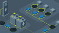
See Figure 5, a Planar/SMD Inverter with Six µMaxPak Switches, on a bottom side cold-plate. The Three output busses are shown as copper strips soldered to each of the three HS & LS pairs of switches. This approach is simple and easy to visualize, but this configuration only takes heat from the bottom side of the µMaxPak switches. It is possible also to remove heat from the three output busses if they are made using DBC substrates for isolation. This configuration increases SiC cooling and performance, but may also increase electrical & thermal interconnect complexity.

Figure 5: Illustration of a Planar/SMD EV Inverter with Six µMaxPak Switches
Although the µMaxPak packages are driven by the performance, efficiency & speed of the SiC switches, they also make extreme reductions to EV & Locomotive Drive size, weight & cooling systems.
About the Author
Courtney Furnival is the president of Semiconductor Packaging Solutions.
This article originally appeared in the Bodo’s Power Systems magazine.