Facebook
 Google
 GitHub
 Linkedin
Mitigating Motor Drive Risks: The Critical Role of Gate Driver Isolation
This article will focus on how a single-point power supply failure can lead to uncontrolled movements and examine how the robust construction of high-voltage optoisolators can mitigate the consequences of power supply failure.
This article is published by EEPower as part of an exclusive digital content partnership with Bodo’s Power Systems.
Functional safety revolves around the assurance that a system will behave predictably and safely, even when faced with internal faults or external disturbances. In motor drives, this entails mitigating risks associated with electrical, mechanical, and software failures. This ensures that the system operates reliably under all foreseeable circumstances and prevents injury, damage, or even loss of life.
This article will focus on how a single-point power supply failure can lead to uncontrolled movements. The other aspect of such failure is the damage to the galvanic insulation barrier, which can lead to electric shock as motor drives deliver high power, operating off AC line high voltages in the range of hundreds to thousands of volts. To minimize the likelihood of accidents and optimize operational efficiency, it will examine how the robust construction of high-voltage optoisolators can mitigate the disastrous consequences of power supply failure.
Image used courtesy of Adobe Stock
Isolator Construction
Before getting into the single-point failure of the power supply, we will look at the construction of an optical and capacitive galvanic isolated gate driver. The reason for focusing on gate drivers is that they are extensively used to drive power semiconductors like IGBTs in motor drives. They provide reinforced galvanic insulation between high-voltage IGBTs and control circuits. Their ability to reject high common mode noise is important to prevent erroneous driving of the IGBTs. Therefore, the robust construction of the isolated gate driver is critical to driving the motor in a fail-safe manner during a fault.
Optoisolators provide reinforced insulation by wide distances through insulation (DTI) between the LED and detector, with three layers of insulation barriers. The three insulation layers are silicone, polyimide film, and silicone, as shown in Figure 1. Polyimide film is developed specifically to withstand the damaging effects of partial discharge, which can cause ionization and breakdown of insulation material. Polyimide’s unique properties of high dielectric strength and wide temperature range allow it to be used extensively in electrical insulation applications, from locomotives to aerospace. The polyimide film used in the ACPL-334J gate drive optocoupler has a typical dielectric strength of 300 kV/mm and can withstand temperatures as low as -200 ºC and as high as 400 ºC. The DTI of ACPL-334J is 0.5 mm.
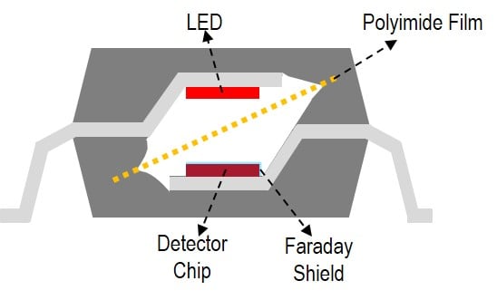
Figure 1. Optoisolator structure with three layers of insulation barrier. Image used courtesy of Bodo’s Power Systems [PDF]
IEC defines a SELV (separated extra-low voltage) circuit as an electrical circuit in which the voltage cannot exceed ELV (extra-low voltage) under normal and single-fault conditions. A SELV circuit must have electrical protective separation from all other circuits. In motor drives, the power supply circuit at the input should be separated from the PWM (Pulse Width Modulation) control circuit. The lead frame at the input of ACPL-334J is designed with a protective separation distance of more than 0.8 mm, as shown in Figure 2.
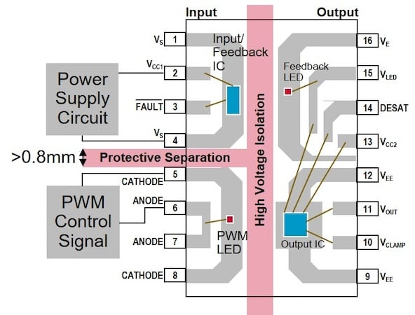
Figure 2. ACPL-334J’s lead frame structure with protective separation. Image used courtesy of Bodo’s Power Systems [PDF]
Capacitive isolators use silicon dioxide (SiO2) as dielectric for the on-chip insulation. The isolation circuit is integrated on the same chip and other circuitry in a monolithic process. High voltage isolation is achieved using two thick SiO2 capacitors in series, one on the input and one on the output sides. The high-voltage capacitors use the same process as the CMOS production. The thickness of the SiO2 or DTI of a capacitive isolator is between 0.014 to 0.028 mm.
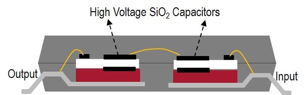
Figure 3. Capacitive isolator structure with two series SiO2 capacitors. Image used courtesy of Bodo’s Power Systems [PDF]
The x-ray of a gate driver using capacitive isolation in a two-chip module is shown in Figure 4. The input and output ICs have isolation capacitors to increase the high voltage capability. As this is a monolithic process, the input IC of the gate driver consists of the power supply circuit, PWM control circuit, and SiO2 capacitor in a single chip.
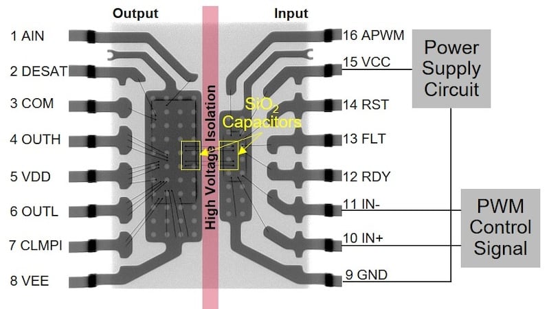
Figure 4. X-ray of a gate driver using capacitive isolation in a two-chip module Image used courtesy of Bodo’s Power Systems [PDF]
A Single Point Failure—Power Supply Fault
One of the primary reasons why functional safety is of utmost importance in motor drives is the catastrophic consequences during faults. A single-point power supply fault can lead to uncontrolled movements and compromise the isolation barrier. On its own, the PWM controller cannot be considered safe off. The reason for this is that if there is a malfunction in the power supply and damage to the input IC, the ability to switch off the motor must be guaranteed.
However, in the single chip architecture of the capacitor isolation, the power supply malfunction can cause input logic (IN+/IN-) to be in the wrong state, signaling wrong motor movements. On the other hand, the lead frame at the input of ACPL-334J provides a protective separation from the malfunctioned power supply. This redundancy in architecture offers a fail-safe condition in which the PWM LED will not transmit the wrong signal to the motor.

Figure 5. Protective separation provides fail-safe conditions during power supply faults. Image used courtesy of Bodo’s Power Systems [PDF]
The other aspect is to study the impact of the power supply fault on the galvanic insulation barrier. A power supply destructive test was conducted by increasing the bias of the supply pins of the optical and capacitive isolated gate drivers until the input IC broke down. This is to simulate the power supply fault with an uncontrolled current surge into the input IC. Per UL 1577, the gate drivers were proof tested by applying an insulation test voltage of 5 kV RMS to detect leakage current, II-O not exceeding 5 µA. Table 1 shows the test conditions and results of the power supply destructive test.
Table 1. High-voltage leakage current test after power supply destructive test
| Power Supply Destructive Test | Input Biasing Conditions before IC Broke Down | II-O, 5kV RMS Per UL 1577 |
| ACPL-334J Control Unit | 3.2μA | |
| ACPL-334J DUT | Anode/Cathode>6V, ILED1>1A(S/C) | 3.2μA (PASS) |
| Capacitive Isolated Gate Driver Control Unit | 1.6μA | |
| Capacitive Isolated Gate Driver DUT | VCC>15V,ICC>13mA | >99.9μA (FAIL tester limit) |
The high-voltage leakage current was applied to a control unit accompanying the device under test (DUT) to see if the insulation barrier was degraded. The ACPL-334J gate driver using optical insulation shows no change in leakage current after the destructive power supply test. This is attributed to the robust insulation construction with wide DTI and the three layers of insulation made up of silicone, polyimide film, and silicone, as shown in the cross-sectional x-ray of ACPL-334J. Although it is obvious that the power supply has damaged the PWM LED and the input IC, the polyimide film or the insulation tape remains unscathed due to its distance from them.
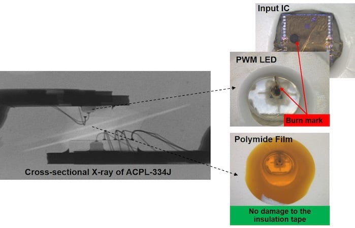
Figure 6. Failure analysis of ACPL-334J after power supply destructive test. Image used courtesy of Bodo’s Power Systems [PDF]
The gate driver using capacitive insulation, however, shows a very high leakage current that exceeds the limit of the high-voltage tester. A failure analysis was conducted to see the extent of the damage that caused the high leakage current.
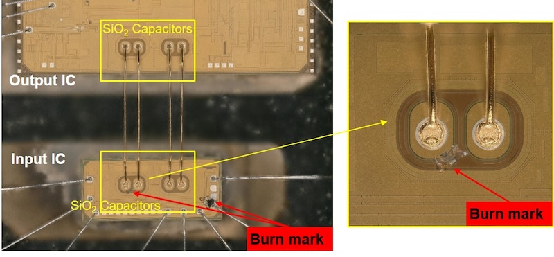
Figure 7. Failure analysis of the capacitive isolated gate driver after power supply destructive test. Image used courtesy of Bodo’s Power Systems [PDF]
Figure 7 shows that the SiO2 capacitor at the input IC is damaged and compromises the insulation capability of the isolator. As the insulation circuit is integrated on the same chip along with input circuitry in a monolithic process, their close proximity and thin DTI are obvious reasons for the failure of the insulation. This shows that the single point failure of the power supply failure can damage the capacitive insulation barrier, which can lead to electric shock and compromise safety.
Optoisolator Takeaways
Both optical and capacitive isolators do a good job insulating high voltage, protecting the low voltage circuit, and ensuring user safety. However, fault events at the peripheral circuit, like the power supply fault discussed here, can damage the insulation barrier, compromising functional and electrical safety. The fundamental construction of the isolation barrier is crucial to determine how easily the fault can reach and damage the insulation barrier. The protective separation in the lead frame and three layers of insulation of the ACPL-334J create a gap impossible for the fault energy to reach. On the other hand, capacitive isolation construction uses a monolithic process, integrating electrical circuits and the SiO2 capacitor in a single chip, creating close proximity for the fault to reach the insulation barrier.
This article originally appeared in Bodo’s Power Systems [PDF] magazine.