 Facebook
 Google
 GitHub
 Linkedin
dV/dt Validation in Motor Drives
dV/dt validation in the motor drives can be applied both during the development process in the lab as well as directly on the end application with the final customer in the field.
This article is published by EEPower as part of an exclusive digital content partnership with Bodo’s Power Systems.
The edge steepness of an inverter can be quickly and practically tested with the oscilloscope without having to manually assess each individual edge in the time domain—dV/dt validation in motor drives—can be applied during the development process in the lab and directly to the end application with the final customer in the field.
Why Is dV/dt Validation Important?
If the edge steepness of the voltage of a motor phase (hereinafter dV/dt) is too high, it can cause damage to the windings through partial discharge in the motor windings. A limit value widely used in the industry is 5 kV/μs. Limit values must be adhered to and checked to protect motors. While this is often performed during the development process with double pulse tests in the lab, this article focuses on the testing of the end application under real operating conditions.

Image used courtesy of Adobe Stock
It is important to understand that there are many different edges within a phase current period. At 50 Hz phase current and 2 kHz switching frequency, there are 80 different edges, including 40 positive and 40 negative. At 16 kHz, there are already 640 edges that need to be assessed for each load condition. Consequently, there is a need for a rapid measurement method because the manual assessment of each individual edge in the time domain is too time-consuming.
The steepness of the edges and their distribution within the phase current period primarily depends on the power semiconductors and their gate resistors. Additional secondary influencing factors include motor load, transient processes during the dead time (soft switching), phase current direction, phase current amplitude, power factor, type of PWM (pulse width modulation), diode snappiness, type and length of the cable, temperature of the semiconductors and the layout of the circuit board and power module.
How Is dV/dt Determined?
The following two parameters are recorded with an oscilloscope:
a) phase current
b) switched phase voltage

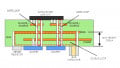
Figure 1. Sketch of measuring points for phase voltage and phase current. Image used courtesy of Bodo’s Power Systems [PDF]
The switched phase voltage is now differentiated and scaled with the help of an oscilloscope math channel. The differentiation transforms the edge steepness from the time domain to the amplitude domain. The scaling standardizes the result to kV/μs.
The transformation into the amplitude domain has the advantage that the result can be directly read on the y-axis. Thus, the laborious assessment of each edge in the time domain is no longer necessary.
Formula for the math channel:
\[\frac{kV}{\mu s}=derivative(Phase\,voltage)\times10^{-9}s\]
It is useful to select the measuring period so that exactly one complete period of the phase current is displayed on the oscilloscope. This means that all edges of a specific operating state can be recorded and mapped in a single shot.
Assessing the Measurement Result
The dV/dt can be read directly from the math channel. It can be seen at a glance whether all edges of a period are within the set limit or whether limit values have been exceeded (green spikes in Figure 2).

Image used courtesy of Bodo’s Power Systems [PDF]

Image used courtesy of Bodo’s Power Systems [PDF]
Figure 2. dV/dt measurement (2.2 kW three-phase asynchronous motor, no-load)
CH1 = Phase voltage against DC
Ch2 = Phase current
MC = dV/dt
If a limit value of 5 kV/μs had been taken as the reference in the above example, it would be immediately seen that this limit value had been significantly exceeded except in the zero-crossing area of the phase current.
Figures 3 and 4 show the close-up shots of an (a) falling and (b) rising edge. You can clearly see how the dV/dt calculation maps the real edge.

Image used courtesy of Bodo’s Power Systems [PDF]

Image used courtesy of Bodo’s Power Systems [PDF]
Figure 3. Falling edge (detail view) (90 W three-phase asynchronous motor, no-load)
Ch1 = Phase voltage against DC
Ch2 = Phase current
MC = dV/dt

Image used courtesy of Bodo’s Power Systems [PDF]

Image used courtesy of Bodo’s Power Systems [PDF]
Figure 4. Rising edge (detail view) (90 W three-phase asynchronous motor, no-load)
CH1 = Phase voltage against DC
Ch2 = Phase current
MC = dV/dt
Edge/IGBT Assignment
If the edge steepness is too high, it must be optimized. In the simplest case, the gate resistors can be adjusted. For optimization, every edge that is too steep must be assigned to the responsible IGBT (insulated-gate bipolar transistor) and its switching direction. In simple terms: You have to know whether the HS (high side) or LS (low side) IGBT is responsible and whether it is currently turning on or off. The assignment requires a case differentiation for (a) the direction of the phase current and (b) the direction of the dV/dt.
The following table lists the correct assignment:
Table 1. Assignment table of the responsible IGBT to the edge. Image used courtesy of Bodo’s Power Systems [PDF]

Figure 5 illustrates the content of the above table in graphical form.

Figure 5. Graphical representation: Assignment of the responsible IGBT to the respective edge. Image used courtesy of Bodo’s Power Systems [PDF]
A practical example is given below. Figure 6 illustrates the assignment of the IGBTs of a flat-top PWM switched inverter.

Image used courtesy of Bodo’s Power Systems [PDF]

Image used courtesy of Bodo’s Power Systems [PDF]
Figure 6. dV/dt measurement (2.2 kW three-phase asynchronous motor, flat-top PWM, load)
Ch1 = Phase voltage against DC
Ch2 = Phase current
MC = dV/dt
Orange arrow: dV/dt = positive & phase current = positive => Turn on HS IGBT
Violet arrow: dV/dt = negative & phase current = negative => Turn on LS IGBT
Turquoise arrow: dV/dt = negative & phase current = positive => Turn off HS IGBT
Green arrow: No edge; i.e., it is a steep-edged capacitative coupling from the neighboring phase.
Note: With fast edges and high capacitive coupling between the motor phases, crosstalk phenomena occur. These are made visible through steep pulses on the phase voltage and, consequently, are also evaluated by the method presented here. However, this is not critical because for physical reasons, the crosstalk phenomena cannot be steeper than the edges themselves. If in doubt, zooming into the measurement will provide information as to whether it is an edge or a crosstalk phenomenon.
Notes on Equivalent Circuit Diagrams in Table 1
Drawing an equivalent circuit diagram for the half-bridge of a phase can simplify the explanation of the commutation behavior because every equivalent circuit diagram contains only one active IGBT. The half-bridge of a phase operates as a BUCK stage if the phase current is positive and as a BOOST stage if the phase current is negative. The half-bridge of a phase can therefore be broken down into two equivalent circuit diagrams, namely into an (a) buck stage and (b) boost stage. In doing so, the diode simulates the anti-parallel diode of the opposite IGBT, which is always conductive during the dead time. (Precondition: non-gap operation, which is almost always present in inverter operation).
Improving Measurement Quality
A number of obstacles must be overcome to achieve a good result because the quality and accuracy of the calculated dV/dt very much depend on the noise of the math channel. It occurs during the calculation and is not signal noise!
Note: The accuracy of the calculated dV/dt is heavily dependent on the noise.
calculated dV/dt = (dV + noise) ÷ dt
For a proper result, the noise must be significantly smaller than the dV/dt of the switching edges (signal-to-noise ratio). It is, therefore, important to know where the noise is coming from and how it can be kept to a minimum.

Figure 7. Notional representation of noise. Image used courtesy of Bodo’s Power Systems [PDF]
Note: Noise can be reduced by (a) higher vertical AD resolution, (b) the smallest possible measuring range, and (c) a lower sampling rate.
The following comparison illustrates how a higher AD resolution and a longer sampling time reduce noise. The following measurement settings are compared:
a) 15-Bit AD resolution / 8 ns sampling time (Figure 8)
b) 8-Bit AD resolution / 2 ns sampling time (Figure 9)
Figure 8 shows that a high AD resolution (15-bit) and a long sampling time (8 ns) result in low noise.

Image used courtesy of Bodo’s Power Systems [PDF]

Image used courtesy of Bodo’s Power Systems [PDF]
Figure 8. Low noise with 15-bit / 8 ns
CH1 = Phase voltage against DC
Ch2 = Phase current (filtered)
MC = dV/dt
Figure 9 shows that a low AD resolution (8-bit) and a short sampling time (2 ns) result in high noise.
The difference in noise is clearly visible. In Figure 9 the noise is even higher than a frequently used limit value (> 5kV/μs) and would thus be unusable for this limit value measurement.

Image used courtesy of Bodo’s Power Systems [PDF]

Image used courtesy of Bodo’s Power Systems [PDF]
Figure 9. High noise with 8-bit / 2 ns
Ch1 = Phase voltage against DC
Ch2 = Phase current (filtered)
MC = dV/dt
Where Is the Noise in the Math Channel From?
The cause is essentially the quantization noise of the oscilloscope’s AD converter. It causes a high-frequency amplitude error. It results in a dV/dt error during the differentiation in the math channel. The noise in the math channel is the sequence of all dV/dt errors and becomes larger the greater the quantization error (AD resolution and measuring range) and the shorter the sampling time (rate).
Choosing a Reasonable Sampling Time
Noise increases and the quality of the result decreases as the sampling rate increases.
It is, therefore, necessary to select a reasonable sampling time. The sampling time must be (a) long enough to keep the noise sufficiently low and (b) short enough to ensure that the edges are sampled with sufficient resolution.
A good compromise is to choose a sampling time that creates about 3 measurement segments (4 samples) within an edge.
For example, the sampling rate should be about 8 ns for a 32 ns edge time (80% / 20%).
This is illustrated in Figure 10. The time between the cursors corresponds to 8 ns and is therefore equal to the sensible sampling time. Three different sections are measured within the edge. The edge is sufficiently well sampled. This is a good compromise between sampling time and noise and results in a good signal-to-noise ratio.

Image used courtesy of Bodo’s Power Systems [PDF]

Image used courtesy of Bodo’s Power Systems [PDF]
Figure 10. Edge length v. sampling time
Ch1 = Phase voltage
Accuracy, Limitations
Of course, this method has its limitations. The calculated edge steepness is always the average value between two measuring points. If there is a steeper section between these points, it will not be detected. However, experiments have shown that good results for a practical, non-scientific assessment can be achieved. This method is less suitable for scientific requirements in which even the smallest partial sections of an edge must be assessed. In this case, every single edge must be sampled with the maximum possible sampling rate and be laboriously assessed in the time domain.
It has been shown that forming the derivative of the phase voltage is a quick, simple, and practical way to assess the edge steepness on the motor drive. It is important to select a reasonable sampling rate, a good vertical resolution, and the smallest possible measuring range.
This article originally appeared in Bodo’s Power Systems [PDF] magazine.


All that, OR you could simply buffer the salient inductance of the 3 phases by 3 small inductors and add a CMC on all three. This isolates the high dV/dt of the switches so that the winding-to winding dV/dt is lower.