Facebook
 Google
 GitHub
 Linkedin
Radiation Performance of Enhancement-Mode GaN Power Devices
Enhancement-mode gallium nitride (eGaN®) technology enables a new generation of power converters in space operating at higher frequencies, higher efficiencies, and greater power densities than ever achievable before. eGaN devices also exhibit superior radiation tolerance compared with silicon MOSFETs.
This article introduces EPC Space’s family of eGaN FETs and ICs which have been specifically designed for critical applications in the high reliability or commercial satellite space environments. Some of the failure mechanisms in GaN and how they impact radiation performance are explored. Lastly, the electrical performance of eGaN transistors is compared with the most popular radiation-hardened (Rad Hard) MOSFETs in the market.
Radiation in Space
There are three primary types of radiation experienced by semiconductors used in space applications. Regardless of whether devices are being employed in satellites orbiting around our earth or incorporated in exploration satellites visiting the most distant parts of our solar system, all experience some form of high-energy radiation bombardment. These types of radiation are gamma radiation, neutron radiation, and heavy-ion bombardment. An energetic particle can cause damage to a semiconductor in fundamentally three ways; it can cause traps in non-conducting layers, it can cause physical damage to the crystal, also called displacement damage, or the particle can generate a cloud of electron-hole pairs that will cause the device to momentarily conduct, and possibly burn out in the process.
In eGaN devices, energetic particles cannot generate momentary short-circuit conditions because mobile hole-electron pairs cannot be generated. Thus, this article will focus on the first two failure mechanisms − trapping and physical damage
Gamma Radiation – Trapping in Silicon MOSFETs
Gamma radiation consists of high energy photons that interact with electrons. Figure 1(a) is a cross section of a typical silicon MOSFET. It is a vertical device with the source and gate on the top surface and the drain on the bottom surface. The gate electrode is separated from the channel region by a thin silicon dioxide layer. In a silicon-based MOSFET, the gamma radiation knocks an electron out of the silicon dioxide layer leaving behind a positively charged ‘trap’ in the gate oxide. The positive charge reduces the threshold voltage of the device until the transistor goes from normally OFF – or enhancement mode – to normally ON, which is a depletion mode state. At this point the system will need a negative voltage to turn the MOSFET OFF. Typical ratings for rad-hard devices range from 100 kRads to 300 kRads. In some cases, devices can be made to go up to 1 MRad, but these tend to be very expensive.
Gamma Radiation – eGaN Transistors
GaN devices are built very differently from silicon MOSFETs. As shown in Figure 1(b), all three terminals; gate, source, and drain, are located on the top surface. As in a silicon MOSFET, conduction between source and drain is modulated by biasing the gate electrode from zero volts to a positive voltage – usually 5 V. Notice that the gate is separated from the underlying channel by an aluminum gallium nitride layer. This layer does not accumulate charge when subjected to gamma radiation.
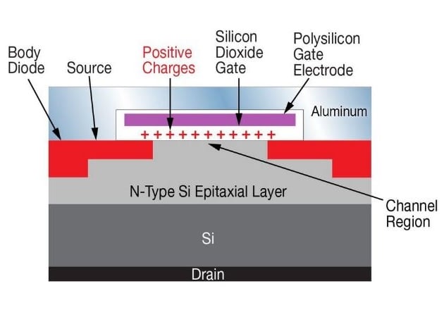
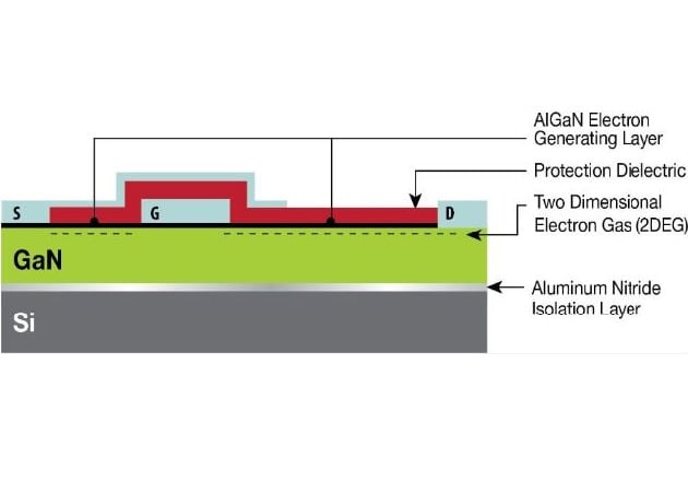
Figure 1: (a) Cross section of a typical silicon MOSFET (b)Cross section of a typical enhancement mode GaN (eGaN®) device
To demonstrate the performance of eGaN devices, EPC Space’s 100 V family of eGaN transistors were subjected to 500 kRad of gamma radiation. Throughout the testing, leakage currents from drain to source and gate to source, as well as the threshold voltage and ON-resistance of the devices at various checkpoints along the way were measured, confirming that there are no significant changes in device performance. Since the initial testing, eGaN devices have been subjected to 50 MRads, confirming that eGaN devices will not be the first part to fail due to gamma radiation in any space system. Testing results are shown in figure 2.
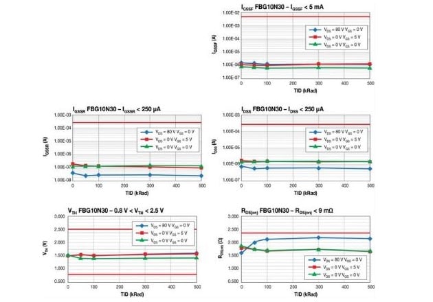
Figure 2: Results of gamma radiation testing of eGaN devices to 500 kRads
Neutron Radiation
The primary failure mechanism for devices under neutron bombardment is displacement damage. High energy neutrons will scatter off atoms in the crystal lattice and leave behind lattice defects. Figure 3 shows the impact of neutron radiation at doses up to 1 x 10¹⁵ per square cm. As with gamma radiation, the impact of neutrons on the GaN crystal and the entire device structure is minimal.
The reason for GaN’s superior performance under neutron radiation is that GaN has a much higher displacement threshold energy compared with silicon.
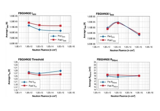
Figure 3: Impact of neutron radiation on eGaN devices at doses up to 1 x 10¹⁵ per square cm
Single Event Effects (SEE) – Si MOSFETs
SEE are caused by heavy ions generated by the impact of galactic cosmic rays, solar particles or energetic neutrons and protons. This can be simulated terrestrially by using a cyclotron to create beams of different ions. Two of the most common ions used to evaluate radiation tolerance of electronics components are Xenon, with a linear energy transfer (LET) of about 50 MeV·cm2/mg, and gold, with an LET of about 85 MeV·cm2/mg.
In a silicon MOSFET there are two primary failure mechanisms caused by these heavy ions, single event gate rupture (SEGR) and single event burnout (SEB). SEGR is caused by the energetic atom causing such a high transient electric field across the gate oxide that the gate oxide ruptures. Whereas, SEB is caused when the energetic particle transverses the drift region of the device where there are relatively high electric fields. The energetic particle loses its energy while generating a large number of hole electron pairs. These hole electron pairs crossing the drift region cause the device to momentarily short circuit between drain and source. This short circuit can either destroy the device, which is a single event burnout, or the device can survive, appearing as a momentary short circuit that can cause damage to other components in the system. This latter case is call single event upset, or SEU.
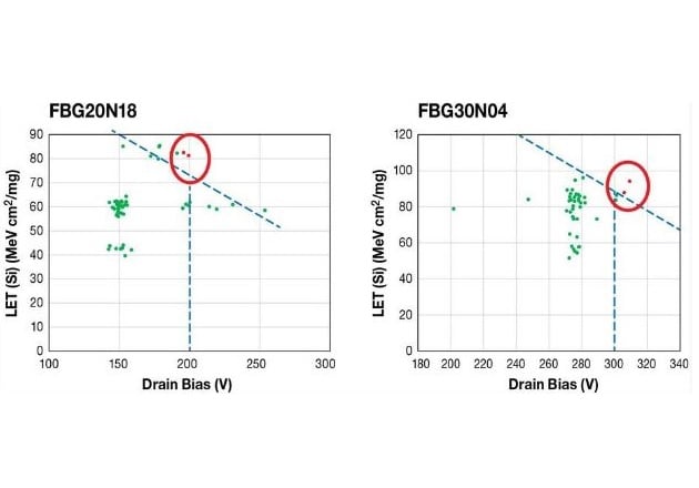
Figure 4: Results from several FBG20N18 200 V products (left) and FBG30N04 300 V products (right)
Single Event – eGaN Devices
Since eGaN devices do not have a gate oxide, they are not prone to single event gate rupture. Also, since eGaN devices do not have the ability to conduct large numbers of holes very efficiently, they are not prone to single event upset. The primary failure mechanism for eGaN devices under heavy ion bombardment is caused by energetic particles crossing the drift region of the device where there are relatively high electric fields. The conditions are about the maximum conditions possible, with an 85 LET beam of gold atoms pummeling the device biased at the maximum data sheet limit. In testing, the gate leakage does not go up during bombardment. The drain-source leakage, however, does start to rise as the displacement damage from the heavy ions increases.
| 100V | Parameter | FBG10N30 | IRHNAG7160 | Units | 200V | Parameter | FBG10N05 | IRHNAG7230 | Units | |
| ID | 30 | 35 | A | ID | 5 | 16 | A | |||
| IDM | 120 | 140 | A | IDM | 40 | 64 | A | |||
| BVDSS | 100 | 100 | V | BVDSS | 100 | 100 | V | |||
| RDS(on) | 9 | 18 | mΩ | RDS(on) | 38 | 130 | mΩ | |||
| QG | 9 | 160 | nC | QG | 2.2 | 50 | nC | |||
| QGD | 2 | 65 | nC | QGD | 0.6 | 20 | nC | |||
| QRR | 0 | 1.9 | µC | QRR | 0.0 | 3 | µC | |||
| RSJC | 2.12 | 0.5 | °C/W | RSJC | 3.6 | 1.67 | °C/W | |||
|
Radiation Level |
>10 M | 300 k | Rad (Si) |
Radiation Level |
>10 M | 300 k | Rad (Si) |
|||
| SEE @85 LET |
100 | 100 | V | SEE @85 LET |
100 | 175 | V | |||
| Size | 23 | 236 | mm2 | Size | 12 | 78.5 | mm2 |
| 100V | Parameter | FBG20N18 | IRHNAG67260 | Units | 200V | Parameter | FBG10N05 | IRHNAG7230 | Units | |
| ID | 18 | 56 | A | ID | 5 | 16 | A | |||
| IDM | 72 | 224 | A | IDM | 40 | 64 | A | |||
| BVDSS | 200 | 200 | V | BVDSS | 100 | 200 | V | |||
| RDS(on) | 26 | 28 | mΩ | RDS(on) | 38 | 130 | mΩ | |||
| QG | 6 | 240 | nC | QG | 2.2 | 50 | nC | |||
| QGD | 1.95 | 60 | nC | QGD | 0.6 | 20 | nC | |||
| QRR | 0 | 11.7 | µC | QRR | 0.0 | 3.5 | µC | |||
| RSJC | 2.12 | 0.5 | °C/W | RSJC | 3.6 | 1.67 | °C/W | |||
|
Radiation Level |
>10 M | 300 k | Rad (Si) |
Radiation Level |
>10 M | 300 k | Rad (Si) |
|||
| SEE @85 LET |
175 | 170 | V | SEE @85 LET |
100 | 170 | V | |||
| Size | 23 | 236 | mm2 | Size | 12 | 78.5 | mm2 |
Table 1: Electrical performance comparisons Rad Hard eGaN transistors against power MOSFETs from Infineon
SEE Safe Operating AreasEPC Space has tested many specially produced EPC eGaN products for SEE under varied conditions. 40 V and 100 V product did not fail under any conditions up to full rated voltage and 87 LET. Figure 4 shows the results from several FBG20N18 200 V products and FBG30N04 300 V products. For the 200 V products, the first failures occurred at 85 LET and 190 V, as shown in the red circle on the left. The FBG30N04 300 V product failed at 85 LET and 310 V as shown in the red circle on the right.
Electrical Performance Comparison
In addition to the superior Rad Hard advantages of gallium nitride over silicon, GaN has superior electrical performance as well. As an example, the electrical performance comparisons of 100 V and 200 V Rad Hard eGaN transistors against Rad Hard power MOSFETs from Infineon are shown in table 1.
The 100 V FBG10N30 packaged part from EPC Space has half the ON-resistance compared to the silicon MOSFET, yet is but one-tenth the size and has about one-twentieth the gate and gate-drain charges that determine switching speed. In addition, the radiation resistance is significantly higher.
At 200 V, the difference in electrical performance of the eGaN transistors is even greater. Note that the eGaN device listed on the left side of the 200 V section of table 1 has similar ON-resistance to its MOSFET counterpart, yet is one-tenth the size, and has about 30 times better switching performance while demonstrating superior radiation resistance.
eGaN Devices for Space
In summary, GaN power transistors and ICs are the best choice for power conversion applications in spaceborne systems. eGaN devices have proven to be more rugged than Rad Hard MOSFETs, when exposed to various forms of radiation. In addition, the electrical performance of eGaN devices is many times superior to the aging silicon power MOSFET.
About the Author
Max Zafrani is the Chief Technical Officer (CTO) of Efficient Power Conversion Space.
Alex Lidow is CEO and co-founder of Efficient Power Conversion (EPC), former CEO of International Rectifier and is the co-inventor of the HEXFET power MOSFET, a power transistor. He has authored numerous peer-reviewed publications on related subjects, and received the 2015 SEMI Award for North America for the commercialization of more efficient power devices. Lidow was one of the lead representatives of the Semiconductor Industry Association (SIA) for the trade negotiations that resulted in the U.S. – Japan Trade Accord of 1986 and testified to Congress on multiple occasions on behalf of the industry.