Facebook
 Google
 GitHub
 Linkedin
Pushing the Limits of GaNbased Power Devices and Power Electronics
This article highlights InRel-NPower exploration of the latest GaN, AlGaN, and AlN semiconductor materials for power electronics applications.
The InRel-NPower research project reaches for maximum power efficiencies in power electronics’ applications by exploring group III Nitride-basing power devices.
Power electronics demands the highest efficiency for converter and inverter applications. Continuous innovation requires the exploration of the latest GaN, AlGaN and AlN semiconductor materials. Within this context, the European Union's Horizon 2020 research and innovation program funded the "InRel-NPower" project (Innovative Reliable Nitride-based Power Devices and Applications) in order to improve functional performance and reliability of nitride-based wide bandgap power semiconductors. Generally, advances in power semiconductor technology address improvements in efficiency, size, weight, and cost of power electronic systems. At present, IGBTs and MOSFETs represent modern switching devices. New components based on wide bandgap materials (SiC and GaN) are on their way to being introduced for the next generation of advanced applications. (1)
As shown in Figures 1 and 2, wide bandgap semiconductors (WBG) such as SiC, GaN, AlN, and diamond show superior material properties when compared to silicon.

Figure 1. Superior material properties of wide band gap semiconductor material in comparison to silicon
The main strategic target of this project is to offer reliable and robust devices processed on GaN-based and AlN-based substrates (available within Europe for high and medium power application), which can help to address important and worldwide relevant social issues including (but not limited to) measures against climate change, sustainability in energy consumption, electrical energy savings, and E-mobility.
Packaging is also carefully addressed in this project, thanks to two innovative packaging solutions that allow the exploitation of the full capability of the GaN material. This requires the combination of the indicated expertise over the stages of the value-chain, paired with a physical understanding of processes and mechanisms acting inside the device. The vision is that this work and the knowledge of the partners involved will help to generate a deeper understanding of the technological issues related to semiconductor devices based on wide-bandgap materials. The target is to bring the European semiconductor value chain partners a step further towards the frontiers of the production and application of robust high and medium power devices.

Figure 2. Superior material properties of wide band gap semiconductor material in comparison to silicon (3, 4)
Whereas the great potential of GaN-based converters have already been demonstrated at the application level, there are still relatively few early adopters of this game-changing technology. The main reasons for this reluctance switch to GaN technology are due to three factors: cost, uncertainty about long-term reliability, and conservatism among power converter circuit designers. InRel-NPower envisions to contribute to the medium to long-term solution of the energy saving issue aspects by providing a clear reliability assessment methodology for GaN, together with convincing and improving device lifetime data, as well as by developing two demonstrators proving the superiority (in terms of efficiency and costs) of the GaN devices developed within this project. In parallel, this project will push the boundaries of WBG technology by studying the implementation of AlN-based technology, which compared to GaN (and any other WBG semiconductor) has even better material properties.
Additionally, it should be emphasized that the nine InRel-NPower EU research partners are completed by two Japanese universities, the University of Mie and the University of Kyushu, as associated research members in a very special EU public funded project structure. The references (5) and (6) as examples provide an insight of their research work, tasks, contributions and results.
Improving Group III-Nitride Semiconductor Compound Material
The activities on the improvement of the GaN epitaxy and material can be roughly split into two parts: improving the HEMT heterostructure that will define the properties of the active device on one hand and the use of different starting substrate materials together with buffer techniques on the other hand.
Due to its physical properties, GaN is probably one of the materials with the potential to develop major importance as a replacement for silicon. However, the maturity of the fabrication processes for the most prominent novel GaN-based devices—the high electron mobility transistors (HEMT)—still needs to improve. The HEMT structures are usually fabricated on silicon wafers with all the physical feedback and consequences a heteroepitaxial system creates. The native freestanding GaN wafers are only negligibly available in small diameter and at high costs. So, the heteroepitaxy on silicon, which is available in large diameters and for a low price, is the most popular choice.
This is physically a more difficult situation, but epitaxy scientists all over the world have developed techniques in metal organic vapor phase epitaxy (MOVPE) for mastering the major problems arising from thermal and structural mismatch of the two materials. Although difficult at this point in time, the growth of GaN-based device structures on silicon works quite successful.
The MOVPE deposition works at relatively high temperatures above 1000°C. Consequently, GaN as the material with a larger coefficient of thermal expansion, shrinks faster than the Si substrate upon cooling the system down to room temperature after growth. As a result, the epitaxial layers experience huge strain and may crack. Additionally, the wafer develops an unfortunate large bow, which is not acceptable for later processing. The advanced epitaxial techniques now allow to introduce complex sequences of strain moderating layers which generate opposite strain states and thereby mitigate the bowing of the wafer.

Figure 3. Mastering the wafer bow in GaN on Si heteroepitaxy.
On the other hand, the silicon substrate and the many hetero-interfaces introduced a large number of misfit dislocations because of the required strain balancing do not match structure wisely. Typically, the dislocations can be drastically reduced over the height of the semiconductor layer stack. However, a remaining dislocation density in the order of 109 cm-2 in the topmost layers remain. It is the electrical behavior of these extended defects (and other point defects) that causes difficulties in the functionality of the devices, reliability, and robustness.
Improving the Reliability of GaN HEMTs and Designing New Device Architectures
Reliability assessments of e-GaN devices play a crucial role in determining long-term stability and functionality. The initial part of these assessments involves understanding the conduction mechanisms under both forward and reverse bias conditions for different ambient temperatures as different gate processing techniques bring about different leakage conduction mechanisms, such as Poole-Frenkel, thermally-assisted tunneling (TAT). As can be seen from Figure 4, Poole-Frenkel is the main conduction mechanism under reverse bias and under forward bias, there are two different conduction models. Between 1.5 V and < 4 V, conduction is basically thermionic emission-based (TE) and for VG > 4V up to breakdown conductions is TAT. Time-dependent dielectric breakdown measurements were done on gate-source diodes on p-GaN-gate based e-GaN devices. Lifetime calculations, shown in Figure 5, indicate a 10-year gate life for VG > 6.5 V at room temperature using the TAT model.

Figure 4. Figure showing the forward and reverse gate leakage characteristics for a typical pGaN gate structure as a function of temperature. Different conduction regimes are indicated.

Figure 5. Operating lifetime prediction under forward-bias conditions at RT and 200C based on thermally assisted tunneling and Poole-Frenkel model. Measured data (blue squares) are in line with the predicted lifetime models.
GaN-on-Si transistors suffer from a poor critical electrical field strength of the Si substrate together with a parasitic conduction at the buffer/ substrate interface leading to device breakdown. That is why the highest reported three-terminal breakdown voltage values for grounded substrate GaN-on-Si HEMTs defined at an off-state leakage current of 1 μA/mm are still below 1.5 kV, which is basically limited by the Si substrate and associated material quality.
In order to suppress the parasitic conduction phenomenon, local Si substrate removal (LSR) was proposed in 2010. The Si substrate removal around the drain electrode enabled electrical isolation of the gate and source from the drain across the buffer layer/Si interface, leading to an enhanced blocking voltage of GaN-on-Si HEMT above 2 kV. Using this method, we recently achieved, for the first time, GaN-on-Si MISHEMTs with LSR under the entire device followed by a backside deposition of the ultra-wide bandgap AlN material (see Figures 6 and 7).
The use of an in-situ SiN gate dielectric combined with the LSR technique together with 15 μm thick AlN layer enabled state-of-the-art GaN-based HEMTs with remarkably low off-state leakage current (<1 μA/mm) up to 3 kV (see Figure 8). The next step is to apply this process to industrial high current (> 10 A) power devices in order to demonstrate the manufacturability of this approach.

Figure 6. Schematic cross-section of AlGaN/GaN MISHEMT after the front side process, the LSR technique, 15 μm thick PVD AlN deposition, and the 2 μm Cu deposition on the back-side.

Figure 7. Optical backside image of the wafer with and without LSR removal patterns, and a 20×500 μm GaN-based MISHEMT after LSR

Figure 8. Evolution of LGD-dependent device breakdown and specific on-resistance (inset) of AlGaN/GaN HEMTs with and without LSR/ thick AlN/Cu by defining the blocking voltage at 1 μA/mm, and off-state leakage current characteristics of AlGaN/GaN MISHEMTs with and without LSR / thick AlN deposition.
Modern Low Inductive Power Module Design for GaN-HEMT
For the module designs, the selected assembly and inter-connection technologies (AIT) have to support maximal the outperformance of the wide-bandgap power semiconductors in use. For instance, this refers to maximum operating junction temperatures, maximal reachable power cycle robustness and enabling a low-inductance module characteristic. Therefore, two promising module concepts with their accompanying design elements—one all ceramics substrate design and one hybrid ceramics-laminate design—are under deeper research investigation.
Due to the necessary cooling performance hotspot management, the common base substrate in both concepts will be a Si3N4-AMB (active metal brazing) substrate. In addition, due to the needed power cycle robustness in hard switching inverter applications, the GaN-chip backside will be attached on this AMB-substrate in both concepts by the Silver sintering technology (sometimes called low temperature joining technology, or LTJT).
Furthermore, one has to notice all three chip terminals – source, gate, and drain – have to be contacted on the chip top side due to its lateral nature as a HEMT device. The selected ‘counter substrate’ and its design has to enable the needed circuitry dissolution for a proper functionality.
All Ceramics Substrates Design
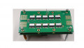
For this concept, the dissolution of the circuitry facing the top side of the GaN-chip will be realized with a multilayer LTCC (low temperature co-fired ceramics) counter substrate (see Figure 9). One very important task is the development of a double-sided Ag-sintering process for the new GaN devices with the die-attach (as the Si-wafer backside) sintered on the AMB and the chip-terminals sintered to the LTCC. The initial trials of applying the Ag-sinter process for LTCC metallization succeeded. (7)
A second important task is the design of the half-bridge. In power mechatronics for power modules in drive inverter applications, the transition from topology and schematics into a concrete power module design in terms sub-components’ and materials’ selection, AIT processes, and their order of implementation in the manufacturing line, is one of the biggest challenges. A rough sketch of this transition for all ceramics module concepts is shown in Figure 9.

Figure 9. Rough sketch of the transition from half-bridge topology to power module design.
Ceramics-Laminate Hybrid Design
Towards the hybrid ceramic-polymer concept a compact interconnection technology replacing conventional wire bonding is being developed. For this purpose, flexible planar metal interconnects on insulating layers are employed, providing the required low inductance and improved thermal management.
The packaging approach includes:
- low inductance interconnects with flexible planar interconnection
- higher frequency drive operation
- compact packaging with higher reliability, robustness, and reduction of system size and
- includes embedded active and passive components, sensors, gate drive unit and cooling
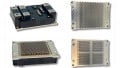
Figure 10 shows a draft of an integrated system applying the innovative planar packaging technology. The ceramic substrate with planar interconnect technology is embedded into a PCB with integrated passives, gate drive unit, and heatsink.

Figure 10. Compact system with planar packaging technology and improved thermal management (3D packaging)
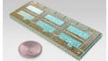
Due to researchers’ resources, the base substrate design strategy uses the same AMB base substrate design and layout in both power module low-inductive concepts described above. Hence, the first step was to define which functional inputs and outputs are needed in principal for the later design flexible AMB substrate layout, e.g., battery plus/minus, phase leg, logical connections, sensing connections, and more. The result of this consideration in terms of the defined AMB layout is shown in Figure 11.

Figure 11. Defined AMB-layout: the planed position of the LTCC counter substrate is shown shaded above the chips.
The second step was to describe the thermal situation under the target characteristics of the new InRel-NPower GaN HEMT (25 mOhm RDS,on channel resistance @ 150°C maximum Tjunction) and the chosen power class of the full B6-bridge demonstrator between 20 up to 30 kW. Due to the small size of the devices, the loss density of the devices is very high. For a proper design of the distance between devices, first simple simulations were carried out with different heat transfer coefficients. The results for a high heat transfer coefficient are shown in Figure 12.

Figure 12. Simulations of two GaN devices in parallel per switch with a variation of distance on a heatsink with high cooling performance.
Summary
We believe that all power electronic systems of the future will take full advantage of the GaN-based and Al-based devices developed within this project. Advantages of doing so include:
- Reduced heat sink requirements, lowering cooling requirements and energy saving;
- 80% reduction in system volume and weight, lowering overall system cost and material usage (due to the much smaller inductors, transformers, and capacitors);
- Lower voltage drop for unipolar devices, lowering conduction losses and saving energy
- Increased output power, leading to more efficient power systems;
- Improved transient characteristics and switching speed, reducing switching losses;
- Reduced electrical noise from smaller system packages, allowing more robust circuits.
This project focuses on the lack in methodology and data by combining the knowledge and expertise of European Centers-of-Excellence in this field and linking it to an EU-based commercial device manufacturer and substrate producers. Doing so allows for the assessment of large-area power devices on a large statistical sample base (rather than focusing on a few R&D samples).
About the Authors
Gaudenzio Meneghesso received the Laurea degree in Electronics Engineering with a major in failure mechanism induced by hot-electrons in GaAs HEMTs and a Ph.D. degree from the University of Padua, Padua, Italy, in 1992 and 1997, respectively. Since 2011, he works as a full-time professor at the University of Padua. His current research interests include electrical characterization and modeling and reliability of semiconductors devices.
Joff Derluyn co-founded EpiGaN in 2010 and currently serves as the Chief Technology Officer. He is driving the R&D activities and is defining the long-term roadmap. Joff is a compound semiconductor process and device expert. Prior to EpiGaN, he worked at imec and was responsible for the III-nitride device characterization and processing. Joff holds an MSc. degree in microelectronics and a Ph.D. from the University of Gent.
Dr. Elke Meissner graduated from the University of Erlangen, Germany, in the field of applied mineralogy. Later she received a PhD from the University of Bayreuth, Germany in the field of analysis of inter diffusion in crystals. Dr. Meissner worked at German universities as well as institutions abroad and recently is a senior scientist in the Department of Crystal Growth at the Fraunhofer Institute of Integrated Systems and Device Technology (IISB). She holds a lectureship at the technical faculty of the University of Erlangen-Nuremberg and is the manager of the Defect Engineering group at Fraunhofer IISB. Dr. Meissner has a broad background in process properties correlation of advanced materials in various fields of crystalline materials. Her recent work is strongly focused on the structural and multi scale characterization of crystals and crystal layers of novel semiconductor materials. Dr. Meissner is inventor or co-inventor of international patents, authored and co-authored numerous papers and contributions to international recognized journals and conferences.
Farid Medjdoub is a CNRS senior scientist and leads the wide bandgap activities at IEMN in France since 2014. He received his Ph.D. in Electrical engineering from the University of Lille in 2004. Then, he moved to the University of Ulm in Germany as a research associate before joining IMEC as a senior scientist in 2008. Multiple state-of-the-art results have been realized in the frame of his work. His research interests are the design, the fabrication, and characterization of innovative GaN-based devices. He is author and co-author of more than 130 papers in this field. He holds several patents deriving from his research. He serves as an Editor for Superlattices and Microstructures journal. He is also a reviewer for various journals and is a TPC member in several conferences. He will be chairing the EuMiC conference within EuMW 2019 that will held in Paris. He is part of the H2020 review panel for the wide bandgap specific calls. Starting from 2019, he will be leading the Nitride power activities within the national French network called GaNex.
Abhishek Banerjee received the Ph.D. degree in electronics engineering from the University of Glasgow, Glasgow, U.K., in 2010.,In 2012, he joined ON Semiconductor, Oudenaarde, Belgium, where he focused on device development and the integration of GaN-based D-Mode and E-Mode devices and assessment of their initial reliability.
Joerg Naundorf works at Siemens AG and is an affiliate of Innovative Reliable Nitride-based Power devices and applications (InRel NPower).
Martin Ritter works at Robert Bosch GmbH and is an affiliate of Innovative Reliable Nitride-based Power devices and applications (InRel NPower).
References
- Wide bandgap semiconductors – Opportunity for power switching devices: wide bandgap semiconductors, website of the InRel- NPower project
- R. Brown, A novel AlGaN/GaN based enhancement-mode high electron mobility transistor with sub-critical barrier thickness, PhD thesis, p. 2, University of Glasgow (2015).
- T. Wunderer et al., Optically pumped UV lasers grown on bulk AlN substrates, Phys. Status Solidi C, 9, 822 (2012).
- H. Okumura, Present Status and Future Prospect of Widegap Semiconductor High-Power Devices, Jpn. J. Appl. Phys., 45, 7565 (2006).
- R. Yoshizawa, H. Miyake and K. Hiramatsu, Effect of thermal annealing on AlN films grown on sputtered AlN templates, Jpn. J. Appl. Phys., 57, 01AD05, 2018.
- P. Kempisty, Y. Kangawa, A. Kusaba, et al., DFT modeling of carbon incorporation in GaN (0001) and GaN (0001 ̅) metal-organic vapor phase epitaxy, Appl. Phys. Lett. 111, 141602 (2017).
- M. Rittner et al., Innovative Reliable Nitride based Power Devices and Applications ‒ The EU Public Funded Project ‘InRel-NPower‘, CIPS 2018 – 10th International Conference on Integrated Power Electronics Systems, Stuttgart, 618 (2018).
This article originally appeared in the Bodo’s Power Systems magazine.