Facebook
 Google
 GitHub
 Linkedin
Pushing GaN FET Performance With Copper Clip Packaging
This article reviews GaN FET technologies and topologies and how GaN FET performance can reach the next level.
Gallium Nitride (GaN) power FETs are increasingly reaching mainstream markets because they offer exceptional efficiency and compact solution size, enabling superior power density in low and high-power conversion applications. The next challenge is pushing GaN FET performance to even higher performance levels by further reducing conduction and switching losses while improving device reliability.

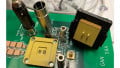
Nexperia’s parallel-connected CCPAK high-power GaN FETs demonstrator board. Image used courtesy of Nexperia
E-Mode and Cascode GaN Switching Performance
High-electron mobility transistors (HEMT) in enhancement mode (e-mode) and cascode variants are today's predominant GaN FET device types. E-mode FETs are normally-off devices (Vth<2 V, VGS=+7 V, -10 V) constructed using a single die. They are better for low-power applications (either low-voltage at higher current levels or high-voltage at low-power levels). However, they come with the caveat of requiring relatively complex drive circuitry because they sometimes require a negative voltage to be turned fully off.
In contrast, cascode FETs are normally-off two-die solutions ideal for high-power applications. They have more robust gate characteristics (Vth = 4 V, VGS= ±20 V), making them easier to drive because they do not require a negative voltage. Materially, the properties of GaN provide it with several advantages in power-switching applications. It has a wider bandgap, higher critical field, and higher electron mobility. Still, unlike Si, GaN has no junctions to deplete, allowing it to switch at the highest frequencies. It also offers the lowest theoretical on-resistance (RDS(on)) for reduced conduction losses.
Power Application Topologies and Landscape
Phase-shifted full bridge (PSFB) and LLC topologies in DC-DC converters, which step down from 400 V to 48 V (for a broad range of telecom applications), benefit from a combination of efficient 650 V cascode devices at the input stage and 100/150 V e-mode devices at the output stage. GaN FETs also enable high-efficiency audio amplifiers and LiDAR for advanced driver assistance systems in automobiles. GaN devices are suited for power factor correction circuitry and inverters in solar photovoltaic and energy storage systems.
Figure 1 shows the application landscape for GaN FETs relative to SiC and Si-based devices. While Si remains a mainstream technology for applications up to 6.5 kV, SiC targets medium and high-power applications from 650 V up to 3.3 kV. GaN targets applications with operating voltage ranges from 80 V to 650 V at the highest switching frequencies.

Figure 1. How GaN fits into the power application landscape. Image used courtesy of Nexperia
How Copper Clip Packaging Improves GaN FET Performance
Copper clip packaging has several advantages over wire-bond packaging, especially in higher-power applications.
High-Current Performance
Copper clip packaging has better current carrying capability due to its bigger clip surface area connecting directly to the die instead of through narrow gauge bond wires. A copper clip allows for better current spreading across the clip rather than small wires that can cause hotspots due to current crowding. Copper clip packaging also reduces device RDS(on) since the contribution of Rpkg is lower than bond wire resistance, which usually must be accounted for in the overall figure. This feature becomes especially relevant when aiming for a total device RDS(on) ≤ 25 mΩ. Finally, wires behave as parasitic inductors that can negatively impact device switching. Copper clip packages inherently have lower parasitic inductance (Lpkg), enabling higher device switching speeds.
Enhanced Structural Reliability
At the board level, copper-clip packages with exposed leads are more reliable than fully enclosed surface-mount packaging (Figure 2) because fully encapsulated pins only permit limited movement in response to changes in temperature and the mechanical stresses caused by vibration. Over time, these can cause cracks in the mold compound or lead to solder joint failure. Hence, copper-clip packages with external leads provide greater flexibility to absorb these stresses, mitigating their impact on the solder joints and mold compound material.

Figure 2. Copper clip offers better reliability than surface mounting. Image used courtesy of Nexperia
Design Topology Support for Increasing Power Levels
The ability to connect multiple GaN FETs in parallel as part of a half-bridge topology is required to satisfy the power levels demanded by the growing number of high-power applications. However, one of the main design challenges is ensuring evenly distributed current sharing between multiple parallel devices while maintaining switching stability. It is crucial for paralleled GaN FETs to share current equally to prevent any individual device from dissipating excessive amounts of power that could compromise its reliability and lifetime. It is also vital that stable switching is maintained without excessive oscillations, which could result in higher than acceptable switching losses.
By using careful layout, short and impedance balanced gate drives, correctly placed DC-bus snubbers, and decoupling, it is possible to achieve excellent current sharing with Nexperia’s 650 V TO-247 led paralleled cascode GaN FETs driving an inductive load on a 4-layer FR4 PCB. Nexperia is now evaluating how to achieve even better performance by connecting up to 5 CCPAK GaN FETs in parallel to achieve current switching above 200 A (for applications exceeding 10 kW of power). The results thus far have aligned with (or exceeded) expectations.
GaN FET Technology and Packaging Takeaways
Nexperia already offers low-power 100 V and 150 V e-mode and 650 V e-mode and cascode GAN FETs in various packages, including TO, DFN, and wafer-level options. These devices offer leading-edge switching performance and efficiency levels for industrial, renewable energy, and telecom applications. Nexperia is transferring over two decades of copper-clip packaging expertise to its GaN device portfolio with the launch of 650 V cascode FETs in gull-wing CCPAK1212 packaging. This unique combination of technology and packaging has the potential to quickly become the industry’s performance benchmark for high-power GaN FETs.
Related Content