Facebook
 Google
 GitHub
 Linkedin
Preventing Start-Up Issues Due to Output Inrush in Switching Converters
This article has shown that careful design of the output filter capacitor is important in designing switching converters.
Switching converters on applications demanding reduced output noise may encounter delayed startup, or may not start up at all, due to excessive output inrush. Output inrush current, attributed to an inappropriate design of output filters and its impact, can be minimized by increasing the soft start time, increasing the switching frequency, or decreasing the output capacitance. In this article, practical design considerations toward preventing start-up issues due to excessive output inrush will be presented.
Many switching converter designs are driven by stringent output noise requirements. The demand for low output noise has pushed designers to implement heavy output filtering, such as using several capacitors at the output. With increased capacitance across the output rail, excessive inrush current may become an issue during startup that can potentially lead to inductor saturation or damage of the power switch.
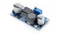
The power switch of a monolithic switching regulator is internal to the chip, as opposed to a switching controller. This is an ideal approach on point-of-load switching converter applications, because of advantages like smaller PCB footprint and better design of the gate-drive circuit. This means that protection against overcurrent becomes a necessity to avoid damaging not only the switch but the regulator chip itself. The ADP5070 dual, high performance dc-to-dc monolithic switching regulator is an example, as illustrated in Figure 1.

Figure 1. Switching converter using ADP5070 regulator
To prevent damage during output overload condition or startup when high current flows through the internal switch, switching regulator manufacturers employ different current-limiting techniques on monolithic switching regulators. Despite the existence of current-limit protection, the switching regulator may not properly operate as intended, especially during startup. For instance, with hiccup mode as the current-limit protection, at initial power-up when the output capacitor is still fully discharged, the switching regulator may enter hiccup mode, causing a longer start-up time or potentially not starting up at all. The output capacitor may pull excessive inrush current that, in addition to the load, causes the inductor current to go high and hit the hiccup mode current-limit threshold.
Overcurrent Protection Schemes
Integrating the power switch inside switching converters makes the current-limiting protection a basic function. Three commonly used current-limiting schemes are constant current-limiting, foldback current-limiting, and hiccup mode current-limiting.
Constant Current-Limiting
For a constant current-limiting scheme, the output current is held constant to a specific value (ILIMIT) when an overload condition occurs. As a result, the output voltage drops. This scheme is implemented by using cycle-by-cycle current-limiting that utilizes the peak inductor current information through the power switch to detect the overload condition.

Figure 2. Cycle-by-cycle constant current-limiting.
Figure 2 shows a typical inductor current of a buck converter during normal and overload conditions for the peak current-limiting scheme. During overload condition, as illustrated by ILIMIT, the switching cycle is terminated when the peak current detected is greater than the predetermined threshold.
In the constant current-limiting scheme, the output current is maintained at ILIMIT, resulting in high power dissipated in the regulator. This power dissipation causes the junction temperature to increase, which may exceed thermal limits.
Foldback Current-Limiting
The foldback current-limiting scheme partially solves the issue with constant current-limiting, helping to keep the transistor in its safe operating area under fault or overload conditions. Figure 3 shows the comparison of the VOUT vs. IOUT response curves between the constant and foldback current-limiting schemes. The reduction in output current (IOUT), as opposed to constant current-limiting, reduces power dissipation, thus reducing the thermal stress on the switching converter.

Figure 3. VOUT vs. IOUT curve of constant and foldback schemes.
The disadvantage of this scheme is that it is not fully self-recoverable. Due to its foldback nature and depending on the nature of the load, the operating point could fall into the foldback region toward the short-circuit operating point once the current-limit threshold was reached or exceeded. This would require power cycling the part or re-enabling the part to get back to the normal operating condition.
Hiccup Mode Current-Limiting
In a hiccup mode current-limiting scheme, the converter switching goes into a series of short burst of pulses followed by sleep time— hence the name hiccup. Once an overload condition occurs, the switching converter enters hiccup mode, where sleep time refers to the switch being turned off for a predefined period of time. At the end of the sleep time, the switching converter attempts to start again from soft start. If the current limit fault is cleared, the device resumes normal operation—otherwise, it re-enters hiccup mode.
The hiccup mode current-limiting scheme overcomes the drawbacks of the two overcurrent protections discussed. Firstly, it solves the thermal dissipation problem, as the sleep time reduces the average load current that allows the converter to cool down. Secondly, it allows smooth autorecovery once the overload condition is removed.
However, some issues may arise if the hiccup mode detector is active during startup. Excessive inrush current, in addition to the load current, may cause the inductor current to go beyond the current limit threshold, which triggers hiccup mode and prevents the converter from starting up. For example, the negative output of the inverting regulator of ADP5071, configured to have an output voltage of –15 V and 100 mA output current with around 63 μF of total output capacitance, is not starting up after powering from a 3.3 V power supply. The negative rail is under hiccup mode, as shown in Figure 4, which is triggered by the large output inrush current. Inductor current peak goes to around 1.5 A, exceeding the typical current-limit threshold of around 1.32 A.

Figure 4. ADP5071 inverting regulator in hiccup mode.
Also, if there’s excessive inrush due to large output capacitance, the converter may get unexpected longer start-up time, as shown in Figure 5.

Figure 5. ADP5070 inverting regulator delayed startup.
Inductor Current in Switching Converters
Inductor Current Average
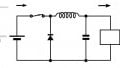
In nonisolated switching converters, the location of the inductor defines the converter topology. With a common ground reference between input and output, there are just three distinct rails possible for the position of the inductor: the input, the output, and the ground rails.
Refer to the three basic switching topologies shown in Figure 6. When the inductor is at the output rail, the topology is a buck. When it is at the input rail, the topology is a boost. And when the inductor is at the ground rail, the topology is an inverting buck-boost.

Figure 6. Basic switching topologies
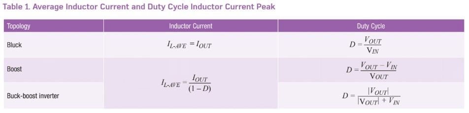
During steady-state condition, the average current (IOUTRAIL) on the output rail must be equal to the output current since the average current on the capacitor is zero. For a buck topology, IL-AVE = IOUT. However, for the boost and the inverting buck-boost topologies, IDAVE = IOUT.
For boost and inverting buck-boost topologies, it is only during switchoff time that current flows through the diode. Therefore, ID-AVE = ILAVE during switch turn off. Refer to Figure 7 in deriving the average inductor current with respect to the output current. The rectangular area in green during switch-off time is the average diode current ID-AVE, with height equal to IL-AVE, and width equal to TOFF. This current all goes to the output and, therefore, can be translated into a rectangular area averaged to a width of T and with height IOUT.
$$I_{L-AVE} \times (T-T_{ON}) = I_{OUT} \times T \ \ \ \ (1)$$
$$I_{L-AVE} = \frac{I_{OUT}}{(1-D)} \ where \ D = \frac{T_{ON}}{T}$$

Figure 7. Diode current of boost or buck-boost inverter.
Table 1 shows a summary of the average inductor current IL-AVE and switching duty cycle D. Based on the equations, the inductor current will be at its maximum when the input voltage is at its minimum providing maximum duty cycle and when the output current is at its maximum.
Inductor Current Peak
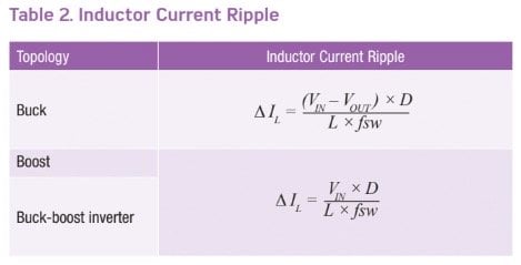
Figure 8 shows inductor voltage and current waveforms of a buckboost inverter in a steady-state condition in continuous conduction mode of operation. As to any switching topology, the amount of inductor current ripple (ΔIL) can be derived according to the ideal inductor Equation 2.

Figure 8. "Swing” of the inductor current.
$$V_L = L \times \frac{dI_L}{dt} \ \ \ \ (2)$$
In switching converter applications where the inductor current is triangular and exhibits a constant rate of change, and therefore constant induced voltage, (ΔIL/Δt) can be used in the inductor equation, as found in the rearranged Equation 3. Inductor current ripple is determined by the applied voltseconds to the inductor and the inductance.
$$\Delta I_{L} = \frac{V_L \times \Delta t}{L} \ \ \ \ (3)$$
Switch turn-on time can be easily related to duty cycle and switching frequency as in Equation 4. It is therefore more convenient to use voltsecond products during switch turn-on than switch turn-off in the succeeding formula.
$$t_{ON} = \frac{t_{ON}}{T} \div \frac{1}{T} = \frac{D}{fsw} \ \ \ \ (4)$$
Table 2 shows a summary of the inductor current ripple in the three different topologies. The voltseconds product term tON, based on Equation 3, is replaced by Equation 4, and the term VL-ON is replaced by the induced voltage across the inductor according to topology.
Looking back at the steady-state inductor current in Figure 8, it will be observed that the inductor current average simply lies at the geometrical center of the ramp or the swinging of waveform at the point ΔIL/2.
Therefore, the inductor current peak is the sum of inductor current average and half of the inductor current ripple, as shown in Equation 5.
$$I_{L-PK} = I_{L-AVE} + \frac{\Delta I_L}{2} \ \ \ \ (5)$$
Capacitor Inrush Current
The charging current or displacement current equation of the capacitor is defined in Equation 6. It states that current flows through a capacitor in correspondence to a rate of change of voltage across it.
$$I_C = C \times \frac{dV_C}{dt} \ \ \ \ (6)$$
The capacitor charging current should be considered when choosing output capacitor values for switching converters. At startup, assuming that the capacitor voltage is equal to zero or no capacitor charge, the output capacitor will begin to charge and draw as much current depending on the total capacitance and rate of change of the capacitor voltage, until the capacitor voltage reaches steady-state.
The rising of the output voltage in switching converters is a controlled ramp with constant slope so the rate of change equation can be simplified, as shown in Equation 7. Change in output voltage (ΔV) corresponds to the output voltage at steady-state and Δt corresponds to the time it takes for the output to reach its final value during startup, or what is commonly called soft start time.
$$I_{CAP} = C_{OUT} \times \frac{\Delta V}{\Delta t} = C_{OUT} \times \frac{V_{OUT}}{t_{SS}} \ \ \ \ (7)$$
If there is too much output capacitance (COUT) or if the soft start time is small, the current demanded from the regulator ICAP may be too high, which may cause problems with the converter operation. This large amount of current impulse is referred to as the inrush current. Figure 9 shows capacitor inrush current and output voltage during the startup of an inverting buck-boost converter with an output of 15 V, 10 μF output capacitor, and 4 ms soft start time.

Figure 9. Output capacitor inrush current.
Inductor Current Peak at Startup
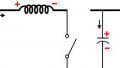
A simple boost converter circuit is shown on Figure 10. When the transistor switch is on close switch, current flows through the inductor while no current flows through the output rail. It is the discharging phase of COUT where the discharging current (ICAP) goes to the output while none goes through the reverse-biased diode. When the transistor’s open switch is off, current ID flows through the diode.

Figure 10. Boost DC-to-DC converter circuit.
By Kirchhoff’s current law, the current through the output rail (ID) must be equal to the sum of the current flowing through the output capacitor (ICAP) and output load (IOUT).
This is described by Equation 8.
$$I_{OUTRAIL} = I_D = I_{CAP} + I_{OUT} \ \ \ \ (8)$$
This equation applies during every charging phase or when voltage is rising across the capacitor. Therefore, it is also applicable during the startup of a switching converter when the initial state of the output capacitor is discharged or when the output voltage is not yet in the steady-state value.
The inductor current peak during startup can be defined using Equation 5 and includes the impact of inrush current due to output capacitor. Equation 8 will be applied into the IL-AVE equations in Table 1, replacing IOUT with IOUT + ICAP. Inductor current peak equations during startup are summarized in Table 3.
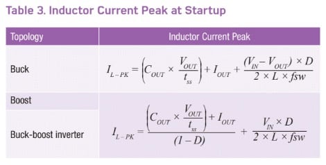
For any of the three topologies, the inductor current peak is proportional to IOUT. In terms of output current, the output capacitor must be designed at full load conditions.
Most applications require operation within a range of input voltage. So against input voltage, there is a difference between the buck and the other two topologies in terms of the magnitude of the dc and ac components voltage of the inductor current. This can be understood better through Figure 11. For the buck, as input voltage goes up, AC component voltage goes up. Average current is equal to output current, so the dc component voltage remains constant. Inductor current peak is therefore maximum at maximum input voltage.

Figure 11. Inductor current against input voltage.
For the boost and buck-boost inverter, as input voltage goes up, ac component voltage goes up—but DC component voltage goes down because of the impact to the average current by the duty cycle, as shown in Table 1. The dc component voltage dominates, so the inductor peak current is at its maximum rating at minimum input voltage. In terms of input voltage, design of the output capacitor must be done at the maximum input voltage for buck and at minimum input voltage for boost and buck-boost inverter.
Mitigating Impact of Inrush
Output Capacitor Filter
As shown in previous sections, too much capacitance at the output causes high inrush current that may cause the inductor current peak to reach the current-limit threshold during startup. Therefore, the right amount of capacitance is necessary to achieve the smallest output voltage ripple, while maintaining good converter start-up performance.
For buck converters, the relationship between COUT and the peak-to-peak voltage ripple is defined by Equation 9.
$$C_{OUT} = \frac{\Delta I_L}{8 \times fsw \times V_{OUT_{ripp_{pk-pk}}}} \ \ \ \ (9)$$
Where:
$$\Delta I_L = \frac{(V_{IN} - V_{OUT} \times D}{fsw \times L}$$
For boost and inverting buck-boost converters, the relationship between COUT and the peak-to-peak ripple is defined by Equation 10.
$$C_{OUT} = \frac{I_{OUT} \times D}{fsw \times V_{OUT_{ripp_{pk-pk}}}} \ \ \ \ (10)$$
Note that these equations neglect the effect of parasitic elements on the capacitors and inductors. These, in line with the rated specifications of the converter, can help the designer in limiting the capacitors added to the output. A good balance of filtering level and output inrush current are key considerations.
Second-Stage LC Filter
In certain cases, switching transients occur on the output voltage, as shown in Figure 12. If the magnitude is significant, it becomes an issue to the output load. The switching spikes are primarily caused by the switching transitions of the current on the output rail, which is the diode current for boost and buck-boost inverters. They can be magnified due to the stray inductance on the PCB copper traces. Because the spikes are in much higher frequency than the switching frequency of the converter, the peak-to-peak ripple cannot be reduced by the output filter capacitor alone—additional filtering is needed.

Figure 12. Output voltage ripple with switching transients.
Figure 12 shows the periodic switching action of the inductor in a boost converter represented by the blue trace, and the output voltage ripple represented by the yellow trace. High-frequency transients are observed within the ripple voltage upon the switching transitions of the inductor current.
A great article on analog.com that provides more insight on how to reduce the high-frequency transients by second-stage LC filtering is “Designing Second Stage Output Filters for Switching Power Supplies” by Kevin Tompsett.
Ripple Measurement
The right measurement method is also important when getting the output voltage ripple. Incorrect measurement setup can result in inaccurate and high voltage ripple readings, potentially leading to over-design of the output capacitor. It is easy to make the mistake of putting too much capacitance at the output in the hopes of reducing voltage ripple without realizing the tradeoffs.
An application note written by Aldrick Limjoco entitled “Measuring Output Ripple and Switching Transients in Switching Regulators” (PDF) should be of help. See the references for details.
Soft Start Feature
For boost and inverting buck-boost, a bigger impact is dictated by the increase of the dc component voltage of the inductor current. At lower input voltage, the increase in the duty cycle causes a big increase in the inductor current average as shown in the (1-D) factor in equations in Table 3—this is also illustrated in Figure 11. This means that the inrush current of the output capacitor has to be significantly reduced. It is achieved by increasing the soft start time (tSS) in Equation 7.
Most switching regulators (tSS) have a soft start feature that refers to its capability, in order to give designers option to adjust the rise time of output voltage during startup. Changing the value of a single resistor is often the convenient method of adjusting the soft start time. Figure 13 shows the start-up waveforms of a buck-boost inverter. A significant 25% decrease in inductor current peak can be seen by a change in soft start time from 4 ms to 16 ms.

Figure 13. Inductor current vs. soft start time.
Increasing the Switching Frequency
Figure 14 illustrates the impact to inductor current by change switching frequency (fSW). Assuming that duty cycle D and output current are constant, the ac component voltage of the inductor current or Δ IL/2 is affected by change in fSW, while the dc component voltage is not. Inductor current peak being inversely proportional is therefore lower at higher switching frequencies.

Figure 14. Factors affecting inductor current peak.
ADP5070: An Example
How Large Can the Output Capacitance Be?
ADP5070 is a monolithic, dual-boost and inverting buck-boost regulator with hiccup mode current-limiting scheme as the overcurrent protection. Some customers forgot to consider the trade-off of putting too much capacitance at the output, especially at high duty cycle operating condition or at the minimum input voltage. This usually has led to start-up issues at the inverting output, because the inverting buck-boost regulator is designed with lower current-limit threshold than the boost regulator.
Figure 15 can be used as aid for application engineers as to how much capacitance is allowed at the output of ADP5070 to avoid startup issues. Max COUT is shown vs. max IOUT on different input and output voltage combinations, using the direct relationship of inductor peak current to output current, including inrush in Table 3’s equation. It will help in the design limits of the output capacitor values after having considered the optimum VOUT ripple performance using either Equation 9 or Equation 10.

Figure 15. Maximum COUT vs. maximum load current.
Both graphs were computed based on the shortest tSS and the current-limit threshold of the regulator. External components were chosen to be of much higher current handling capability than the regulator. In other words, the numbers in these graphs will definitely increase in magnitude if the tSS were increased.
For applications requiring higher output load current, ADP5071 should be considered. ADP5071 is designed with higher current-limit threshold than ADP5070 for both boost and inverting buck-boost regulators.
Computed vs. Measured Data
Figure 16 shows the start-up waveforms of the inductor induced voltage and current of the inverting regulator, while the data that follows in Figure 17 show the inductor current data both by computation using equation in Table 3 and measured bench data.

Figure 16. Inductor current and induced voltage at startup.

Figure 17. Inductor current: computed vs. measured.
The data proves that inrush current is greatly reduced if tSS is increased, thereby lowering inductor peak current. At 4 ms tSS, the inverting regulator is already hitting the current-limit threshold of 0.6 A and has a tendency of having start-up issues. The remedy is to increase tSS to 16 ms to give enough inductor peak current margin.
The Importance of the Output Filter Capacitor's Design
This article has shown that careful design of the output filter capacitor is important in designing switching converters. Good knowledge of the factors influencing the inductor peak current during startup helps avoid start-up issues. Boost and inverting buck-boost converters are more prone to these issues, especially those using the hiccup mode current-limiting scheme.
A direct relationship between the inductor peak current and output inrush current has been provided. It will prove to be useful when designing the output capacitors while keeping track of the inductor peak current against the current-limit threshold. For the same output conditions, output inrush current can be minimized by increasing the soft start time or the converter switching frequency.
This article comes as a reference material when designing a DC-to-DC switching converter using the ADP5070/ADP5071/ADP5073/ ADP5074/ADP5075 series of monolithic switching regulators of Analog Devices.
About the Author
Fil Paulo Balat holds a Bachelor's Degree in Electrical and Electronics Engineering at Xavier University. He is a professional with more than 15 years of progressive experience in power supply design and product development. He currently works as a Staff System Applications Engineer at Analog Devices since August 2016.
Jefferson Eco holds a Master's Degree and Bachelor's Degree in Electronics Engineering at Mapua Institute of Technology and Camarines Sur Polytechnic Colleges respectively. He currently works as an Applications Development Engineer at Analog Devices; Focusing on power supply noise mitigation and load sensitivity evaluation.
James Jasper Macasaet holds a Master's Degree and a Bachelor's Degree in Electronics Engineering at Mapua Institute of Technology and at the University of Santo Tomas respectively. He is currently working as an Applications Engineer at Analog Devices since March 2017.
References
- Erickson, R.B. and D. Maksimovic. Fundamentals of Power Electronics, Second Edition. Springer, 2001.
- Kirchhoff, Gustav. “Kirchoff’s Current Law.” Electronic Tutorials.
- Limjoco, Aldrick S. Application Note AN-1144 Measuring Output Ripple and Switching Transients in Switching Regulators. Analog Devices, Inc., January 2013.
- Tompsett, Kevin. “Designing Second Stage Output Filters for Switching Power Supplies.” Analog Devices, Inc., February 2016.
This article originally appeared in the Bodo’s Power Systems magazine.