Facebook
 Google
 GitHub
 Linkedin
Powering the Future: IGBTs Boost Renewables
Insulated Gate Bipolar Transistor technology is crucial for high efficiency in high-power applications, especially where blocking voltages are above 600 V.
This article is published by EEPower as part of an exclusive digital content partnership with Bodo’s Power Systems.
Insulated Gate Bipolar Transistor (IGBT) technology is crucial for high efficiency in high-power applications, especially with blocking voltages above 600 V.
Renewable energy sectors, such as photovoltaic (PV) and energy storage systems (ESS), have grown significantly in combating global warming, driving up the demand for power semiconductors. The demand for inverters with high power ratings is increasing. Engineers must design high-power systems within a limited space, necessitating IGBT modules that deliver higher output power while maintaining established package sizes. The Low-Voltage Directive 2014/35/EU allows a voltage level of up to 1500 V DC for “low-voltage” applications. The 1200 V-class IGBT power modules are vital in these systems as it is possible to develop a 3L-ANPC (three-level Active Neutral Point Clamped) topology to address the requirement of DC-Link voltages of up to 1500 V.

Image used courtesy of Adobe Stock
Increasing the power density per power module is considered an important target for achieving higher output currents while using the 1200 V IGBT modules, especially for high-power solar or energy storage converters requiring the 3L-ANPC topology where there are certain cost implications for the efforts needed for cooling. This requires reducing electrical losses to optimize efficiency and improving heat dissipation to operate at higher power levels without overheating, ensuring reliability and performance.
Performance Estimation and Design Targets
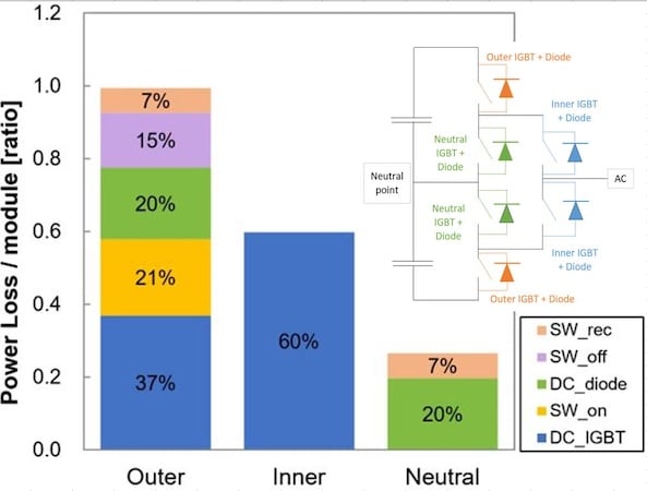
Figure 1. The power loss distribution by using of conventional 1200 V class module. Conditions: Tvj=150 °C, Vcc=750 V, M=0.75, PF=1, fc=3 kHz, fo=50 Hz, 3-level A-NPC topology. Image used courtesy of Bodo’s Power Systems [PDF]
Figure 1 illustrates the normalized ratio of calculated conduction and switching losses for the 7th generation 1200 A/1200 V rated IGBT product in an LV100 package considering the 3L-ANPC topology. In the figure, conduction losses and switching losses are referred to as DC and SW, respectively.
The losses are dominated by the DC power losses. This is true for IGBT and diode and for all devices: outer, inner, and neutral. Additionally, the turn-on switching power loss ratio is particularly pronounced in the outer devices. Therefore, targeted reductions in IGBT DC power losses, diode DC power losses, and turn-on switching power losses are critical for minimizing total power losses within the system.
Reducing these specific power losses can substantially enhance the overall system efficiency. The high DC power loss rates in the IGBT and diode suggest that optimization in these components could yield significant performance improvements. Similarly, addressing the elevated turn-on switching power losses at the outer devices can further contribute to a decrease in total power dissipation, enhancing the module’s operational efficiency and reliability.
8th Generation Chip Technology – Key Features
Mitsubishi Electric’s 8th generation IGBT chips primarily utilize the Split-Dummy-Active (SDA) gate structure and the Controlling-Charge-Carrier-Plasma-Layer (CPL) structure. These advanced technologies are described in this article in detail.
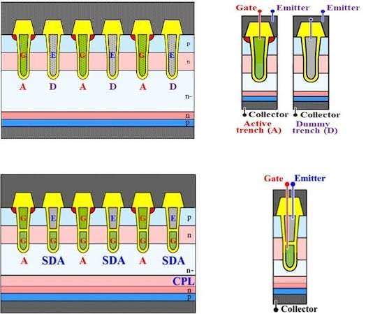
Figure 2. Chip cross-section of 7th generation CSTBT (top) vs. 8th generation CSTBT (bottom). Image used courtesy of Bodo’s Power Systems [PDF]
In Figure 2, schematic cross-sectional views of the 7th generation and the 8th generation involving SDA and CPL are presented.
Turn-on switching power loss in IGBT modules can be reduced through high-speed switching, but this results in high reverse recovery dv/dt, which generates EMI and stresses motor insulation.
To manage this, gate resistance (RG) is typically increased, but this also increases switching power losses. Therefore, reducing reverse recovery dv/dt without increasing RG is crucial.
The 8th generation uses SDA trenches instead of dummy trenches. In SDA trenches, the upper electrode connects to the emitter and the lower electrode to the gate. Additionally, a CPL structure is applied to the backside buffer.
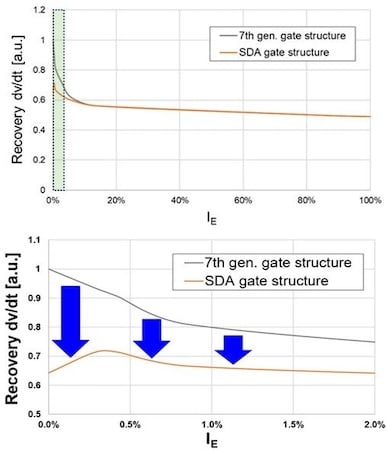
Figure 3. Chip characteristics. Emitter current dependence of recovery dv/dt. 0-100% area on top; 0-2% area on bottom. Image used courtesy of Bodo’s Power Systems [PDF]
Figure 3 depicts the emitter current (IE) dependence of reverse recovery dv/dt for both generations. The SDA structure increases gate-collector capacitance (CGC) without affecting gate-emitter capacitance (CGE), effectively reducing recovery dv/dt at low currents without impacting high currents. This is critical as reverse recovery dv/dt is typically highest at low collector currents.
Decreasing chip thickness can reduce DC and switching power losses, but this must be balanced with breakdown voltage considerations. During high di/dt turn-off operations, excessive VCE surge voltage can destroy the IGBT. Suppressing the turn-off VCE surge voltage is essential for reducing chip thickness and enabling high di/dt operation.
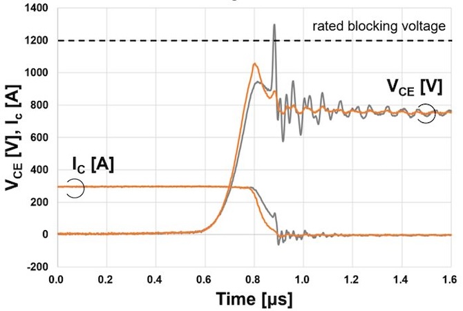
Figure 4. Turn-off waveforms of the IGBTs with and without CPL. Condition : Tvj=150 °C, Vcc=750 V, VGE=15 V, RG=1.6 Ω, IC=rated current. Image used courtesy of Bodo’s Power Systems [PDF]
The 8th generation IGBT uses an optimized backside buffer with a Controlling Charge Carrier Plasma Layer CPL structure. The CPL structure enhances turn-off softness by managing the distribution of charge carriers during turn-off, thereby reducing peak VCE surge voltage and oscillations. Figure 4 illustrates that the IGBT with CPL suppresses turn-off VCE surge voltage below the 1200 V rating, unlike the sharp surge observed in IGBTs without CPL.
This improved design allows for higher di/dt turn-off operations, reduced chip thickness, and consequently lower power losses, making the 8th generation IGBT more efficient and reliable.
In the following, a benchmark is performed to quantify the advantages of the 8th-generation chips and their advanced technologies, including the SDA gate structure and the CPL.

Figure 5. 1200V-class chip area and Rth(j-c). Image used courtesy of Bodo’s Power Systems [PDF]
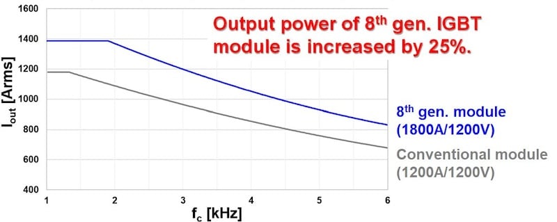
Figure 6. Output power comparison. Condition : Tvj=150 °C, Vcc=750 V, M=0.75, PF=1, fo=50 Hz, forced air cooling, Ta=40 °C, 3-level A-NPC topology. Image used courtesy of Bodo’s Power Systems [PDF]
The 8th Generation Chip Technology – Performance Benchmarking
Figure 5 illustrates the chip areas and a normalized comparison of junction-case thermal resistance (Rth(j-c)). The 8th generation 1200 V-class chips are optimized for the LV100-package chip mounting areas. By increasing the IGBT chip area by 39% compared to the 7th generation, the 8th generation IGBT significantly reduces Rth(j-c) and DC power loss.
The 8th generation diode, optimized for loss trade-offs and chip thickness, also benefits from an 18% larger chip area than its predecessor. This expansion reduces both, Rth(j-c) and DC power loss. Additionally, the internal design of the LV100 package has been optimized to maximize the chip mounting area for the 8th-generation IGBT modules.
As a result, Figure 6 illustrates the relationship between carrier frequency (fc) and output current (Iout) of the IGBT modules. The horizontal axis represents fc, while the vertical axis shows the running value of Iout. The results indicate that the 8th generation IGBT module can achieve approximately 25% more output power than conventional modules. Alternatively, carrier frequency could be increased from 2.7 kHz to 4.4 kHz for the same output power.
Advanced Technology of IGBT Chips
The 8th generation IGBT chips, utilizing advanced technologies such as the Split-Dummy-Active gate structure and Controlling Charge Carrier Plasma Layer structure, represent a significant leap in Si IGBT chip technology. These innovations enhance power density, reduce switching and DC power losses, and improve thermal performance.
The renewable energy sectors, particularly photovoltaic (PV) and energy storage systems (ESS), have driven increased demand for high-efficiency power semiconductors. The 1200 V-class IGBT modules, crucial in these applications, benefit from higher output power capabilities while maintaining conventional package sizes. The 8th generation chips achieve this by optimizing chip thickness, enhancing the backside buffer design, and expanding chip areas within the LV100 package.
Testing has demonstrated that the 8th generation IGBT modules significantly reduce switching losses and improve thermal performance compared to previous generations. Figures show a 39% increase in IGBT chip area and an 18% increase in diode chip area, leading to reduced junction-case thermal resistance (Rth(j-c)) and DC power losses. Additionally, these modules achieve approximately 25% more output power, with further potential improvements through optimized cooling and system design.
The 8th generation IGBT modules offer substantial advancements in efficiency, reliability, and power density, making them ideal for high-power applications in rapidly growing renewable energy markets.
This article originally appeared in Bodo’s Power Systems [PDF] magazine and is co-authored by Narender Lakshmanan and Eugen Stumpf of Mitsubishi Electric Europe B.V., Ratingen, Germany, and Daichi Otori, Mitsubishi Electric Corporation, Fukuoka, Japan.