Facebook
 Google
 GitHub
 Linkedin
PCB Embedding of Semiconductor Dies: Enabling Next-Gen Power Electronics
The embedding of semiconductor dies, particularly GaN and SiC MOSFETs, into PCB structures provides multiple system-level benefits. Learn how this advanced packaging technique improves performance.
This article is published by EEPower as part of an exclusive digital content partnership with Bodo’s Power Systems.
Article co-authored by Simon Stringer, Power Electronics Consultant at Gipfel EDS.
With reduced parasitics and improved thermal management, power converters can operate at higher efficiencies and power densities. The ability to push semiconductor devices closer to their absolute maximum ratings, as specified in their datasheets, allows for better utilization of their capabilities. These improvements lead to lower energy consumption, reduced heat generation, and more compact and cost-effective power electronic solutions.
Optimized Layouts for High-Speed Switching
Embedding semiconductor dies within a PCB enables a more compact and optimized circuit layout, drastically reducing power loop inductances and associated parasitic effects. This reduction is crucial for achieving faster switching speeds without the risk of excessive switch node ringing.
In conventional PCB designs, external packaging and wire bonding introduce inductive parasitics that limit switching performance and can lead to voltage overshoot. By embedding the die directly into the PCB, designers can minimize these detrimental effects and unlock the full high-frequency potential of wide-bandgap semiconductors.

Figure 1. Embedding unlocks the “z-axis,” allowing components to be placed vertically and reducing power loop parasitic inductances. Image used courtesy of Bodo’s Power Systems [PDF]
Thermal Management with Embedded Ceramic Tiles
One of the key advantages of die embedding is the ability to integrate a ceramic AlN (aluminium nitride) tile within the PCB, onto which the die is sintered. AlN provides excellent thermal conductivity while maintaining electrical isolation, ensuring efficient heat dissipation from the semiconductor device. This method effectively reduces thermal resistance, allowing the embedded MOSFETs to operate at higher power levels without excessive temperature rise, improving reliability and longevity.
Improved Clearance and Creepage for Higher Power Density
By embedding semiconductor dies, the pollution degree of the environment is effectively reduced, allowing for more relaxed clearance and creepage requirements. This means that dies can be placed closer together, increasing overall power density. The compact arrangement enables more efficient power conversion in applications requiring high power output within a small footprint, such as automotive and aerospace power electronics.
Unlocking 3D Circuit Design Capabilities
Traditional PCB layouts are constrained to a two-dimensional plane, limiting circuit optimization. With embedded dies, the design paradigm shifts to a three-dimensional approach where the z-axis becomes available for further enhancements. High-frequency ceramic decoupling capacitors can be placed directly on top of the embedded die, minimizing the power loop, and improving transient response. Similarly, shunt resistors for current sensing can be positioned directly atop the die, significantly reducing parasitic inductance, and enhancing signal integrity for precise current measurement.
Reliability and Mechanical Integrity
Embedding reduces mechanical stresses on semiconductor dies by eliminating traditional wire bonding, which can be a common point of failure due to vibration and thermal cycling. Enhanced mechanical robustness makes embedded power modules ideal for harsh environments such as automotive, aerospace, and industrial applications.
Integration of Current Sensors, Gate Drive and Protection Circuitry
Embedding allows for the co-packaging of current sensors, gate drivers and protection circuits (such as overcurrent and overtemperature protection) close to the power switches, minimizing delays and improving switching performance. This tight integration enhances system reliability and further reduces parasitic effects.
Reduction of EMI and Noise
The shorter interconnects and reduced loop areas lead to significantly lower electromagnetic interference (EMI), improving compliance with EMC regulations. This allows for simpler filtering requirements, reducing the need for bulky and expensive external components.
Advanced Manufacturing Techniques and Challenges
Manufacturing methods such as laser drilling, sequential lamination, and sintering enable reliable embedding. However, challenges such as yield rates, thermal expansion mismatches, and inspection/testing difficulties compared to traditional PCB manufacturing must be addressed.
Impact on System Cost and Manufacturing Scalability
While embedding increases initial manufacturing complexity, it can reduce overall system costs by eliminating bulky heat sinks, reducing PCB layers, and minimizing external packaging requirements. This technology’s scalability for mass production is improving as advancements in PCB manufacturing make it more accessible.
RAM Innovations
With a focus on advanced solutions for wide band gap semiconductors in power applications, RAM Innovations concentrates on heterogeneous PCB embedded die packaging, which means that bare die WBG semiconductors are embedded directly within PCBs—rather than mounting them on the surface. This reduces power loop lengths, minimises parasitic inductance, enhances circuit efficiency, lowers energy consumption, and significantly reduces module size and weight—critical advantages across a wide range of high-performance applications.
While optimised for WBG semiconductors, the technology also supports embedded magnetics, RF, and optoelectronic dies. Applications span automotive, aerospace, space, defence, and medical sectors, where the inherent EMI shielding and reliability of embedded packaging are particularly advantageous.
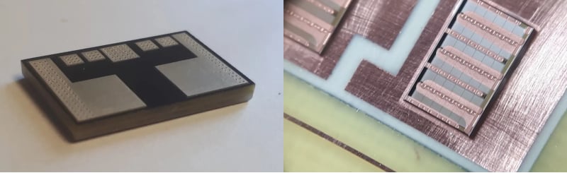
Figure 2. Example of RAM’s embedded power modules. Image used courtesy of Bodo’s Power Systems [PDF]
The GT1 Power Module
A first demonstrator product is a 100 V/90 A half-bridge power module featuring an embedded GaN die (100 V, 7 mΩ). The module also includes an embedded AIN ceramic tile onto which the GaN dies are silver sintered. The AIN ceramic provides galvanic isolation and a low thermal resistance path to an external heat sink. Additionally, embedded copper terminals are also included for a low electrical resistance path from the DC bus and the switching phase to the GaN die.
The GT1 half-bridge module includes self-powered galvanically isolated gate drivers and DC link decoupling capacitors. The capacitors are directly placed above the GaN die in order to lower the impedance path to the GaN die. This can only be achieved with embedding as it unlocks the z-axis.
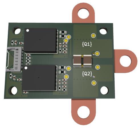
Figure 3. The GT1 Power module with embedded 100 V/7 mΩ GaN die. Image used courtesy of Bodo’s Power Systems [PDF]
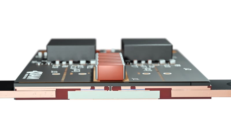
Figure 4. Cross section render of the GT1 Power Module. Image used courtesy of Bodo’s Power Systems [PDF]
Test Boards and Evaluation
Two 500 W buck 48 V-to-12 V DC/DC converters using 100 V/ 7 mΩ GaN devices demonstrate the effectiveness of PCB embedding of power semiconductors compared to traditional surface mount designs. One design utilizes the GT1 half-bridge power module and other uses discrete packages that are surface mounted.
This shows that more power can be obtained from a circuit with embedded components and an AIN ceramic tile, offering higher power densities in a given volume. This is because embedding results in lower thermal resistance from die to ambient, which means that the temperature can be closer to the heatsink temperature whilst also providing galvanic isolation. Additionally, embedding reduces parasitic inductance, resulting in switching waveforms with sharper rise and fall times with less ringing. This lower switching loss and allows for reliable and efficient operation at higher switching frequencies.
To perform an “apples to apples” comparison, the DC/DC converters for both embedded and non-embedded design share the same input and output decoupling capacitors, power inductor and heatsink. Both are designed to convert 48 V to 12 V at up 20 A of load current at a switching frequency of 500 kHz.
The discrete version is designed using best layout practices to minimise as much as possible the parasitic inductances of the power loops. Notice that for the design with discrete GaN, thick thermal pads are required to provide electrical isolation. This increases the thermal resistance and will consequently limit the amount of power that can be obtained; this is the main limitation of using discrete surface mount devices.
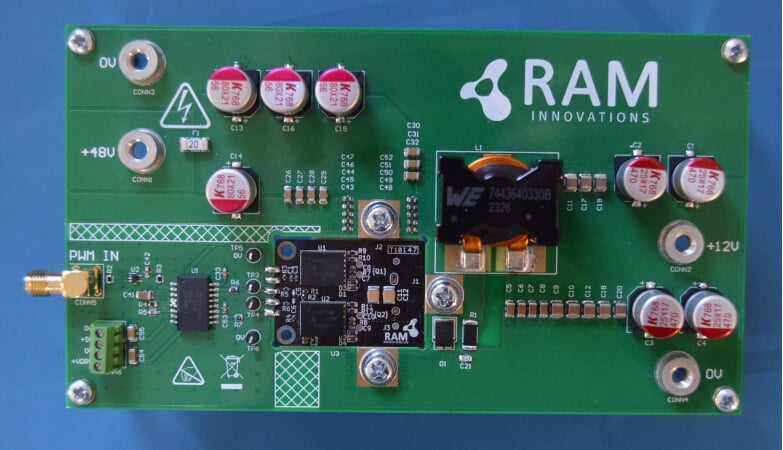
Figure 5. DC/DC Converter with RAM’s GT1 Half-Bridge GaN module. Image used courtesy of Bodo’s Power Systems [PDF]
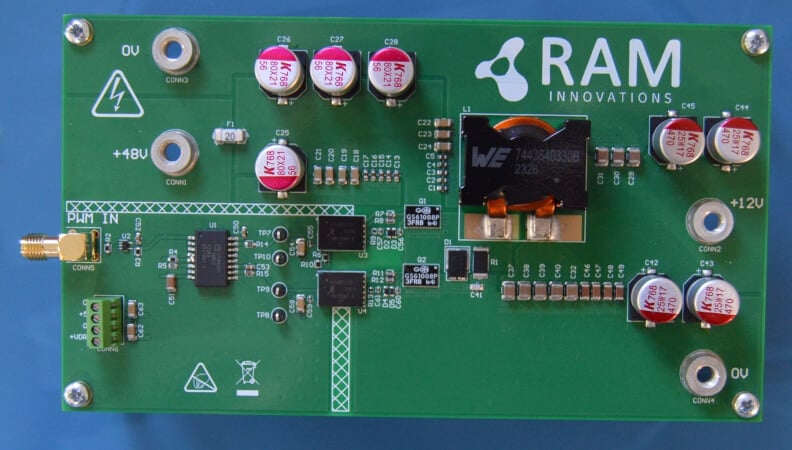
Figure 6. DC/DC Converter using traditional surface GaN components. Image used courtesy of Bodo’s Power Systems [PDF]
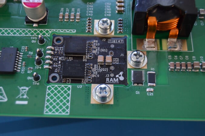
Figure 7. Close-up of the installed GT1 GaN Half-Bridge Module. Image used courtesy of Bodo’s Power Systems [PDF]
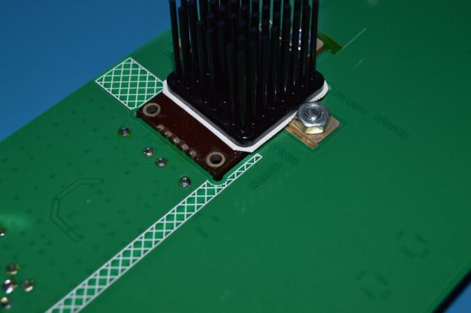
Figure 8. Heatsink attachment for both board designs. Image used courtesy of Bodo’s Power Systems [PDF]

Figure 9. GT1 Module turn-off switching waveform. Image used courtesy of Bodo’s Power Systems [PDF]
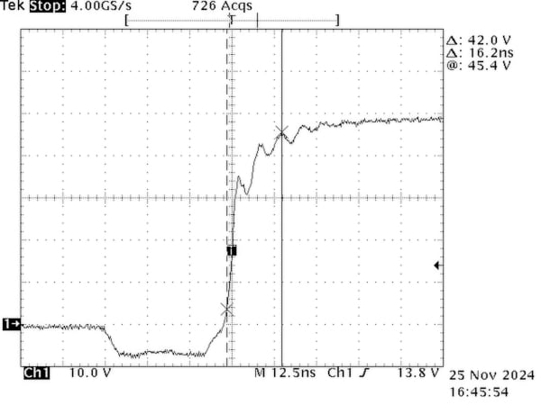
Figure 10. Discrete design turn-ff switching waveform. Image used courtesy of Bodo’s Power Systems [PDF]
Switching Waveforms
The first result to compare is the switching node waveform at turn-on and turn-off. With embedding it is expected to have less parasitic inductance in the power loop so the switching waveform should have little to no ringing, overshoots and undershoots. For this comparison, both designs are operating at approximately 17 A of load current at 500 kHz switching frequency.
The images 9 and 10 show how the turn-off switching waveform of the GT1 half-bridge module provides a clean and smooth rise of the voltage and turn-off. Whereas the turn-off switching waveform of the design with the discrete design shows higher frequency ringing and oscillation riding along the waveform. The consequence of better switching waveforms is that better EMC performance and less noise can be expected. This, in turn, will impact the entire system as fewer filtering components are needed.
Maximum Load Current & Efficiency
Next comparison is the efficiency versus load current, here we would expect the efficiency to be almost identical between the two designs. The curves below show how the efficiency varies with load current for the two designs, the difference between both curves is negligible or within margin of error of the measurement equipment and operating parameters.
For the discrete solution, the maximum achievable load current was approximately 15 A at 12 V before reaching the thermal limit of the discrete GaN devices. There was a temperature of approximately 131 °C on the low-side GaN device, and the heatsink reached a temperature of 84 °C. This means there is a temperature difference of approximately 47 °C between the GaN device and the heatsink indicating a large thermal resistance.
Whereas for the GT1 Module the maximum load current that was achieved was approximately 17 A at 12 V – with a surface temperature of 134 °C and the heatsink reached a temperature of 120 °C. It was expected that the actual temperature of the embedded die would be slightly higher than 134 °C, however, the heatsink temperature was just 120 °C which is only 14 °C lower than the topside of the module.
This result confirms that the low thermal resistance achievable with embedding along with RAM’s patented LAC technology, the die temperature can be closer to the heatsink temperature which therefore allows the system to deliver more power compared to discrete GaN solution with the same thermal and heatsinks. Since the volumes of the two solutions are the same and power is proportional to current squared this already represents a 27 % improvement in power density.
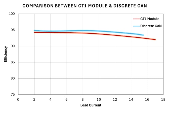
Figure 11. Efficiency comparison between GT1 module and discrete GaN at 12 V output. Image used courtesy of Bodo’s Power Systems [PDF]
The result above shows that the embedded design still has the capability to deliver more output power if the thermal design is changed and optimised. As mentioned previously, since the embedded GaN dies are galvanically isolated due to the internal AIN tile, there is no need for a thermal interface or pad from the surface of the power module to the heatsink, and so a large copper standoff can be used to interface the module to the heatsink and therefore the total thermal resistance can be reduced significantly.
Additionally, since the heatsink that was used did have a temperature of 120 °C which was close to the surface temperature of the module, this means a larger heatsink can be used to allow for more power dissipation.
Figure 12 shows that the GT module is now able to deliver up 36 A of output current with the optimised thermal design using die embedding and the internal galvanic isolation.
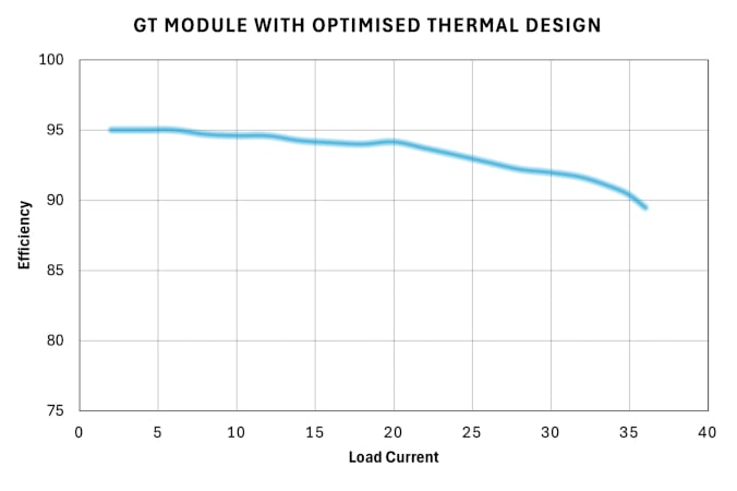
Figure 12. Efficiency measurement of the GT1 module at higher loads. Image used courtesy of Bodo’s Power Systems [PDF]
Maximum Power Dissipation and Current Evaluation
Embedding and the LAC technology allow for lower electric impedance and thermal resistances to be achieved, thus allowing power semiconductors to operate closer to their absolute maximum ratings as specified in their datasheets. To test the absolute maximum current and power ratings of the GT1 Module, a water-cooling setup with a heat exchanger mounted to the bottom side of the GT1 Module was attached for heat extraction, and both, the top and the bottom embedded die, were turned on at gate voltage of 5 V.
A current limited power supply was used to conduct current through both dies and the surface temperature was monitored continuously. Image 13 shows the cooling setup for this single test, and Figure 14 shows the absolute surface temperature rise of the GT1 module whilst conducting a constant current of 55 A. The voltage drop measured directly across the positive and negative terminals was 1.992 V indicating a power dissipation of approximately 110 W. It is expected that both dies will have equal power dissipation of 55 W.
Since the GaN dies are embedded inside the PCB structure, it might not be feasible to measure their temperature directly. By referring to the manufacturer’s datasheet it is estimated that under the operation conditions of this specific test and the cooling setup the junction temperature of the dies has reached approximately 150 °C.
The initial estimates, based on these preliminary tests and FEM simulation, were that the thermal resistance from the embedded die to the bottom surface of the GT1 Module is 0.2-0.4 °C/W. The next product generation of the GT1 Module will include an embedded thermistor which will provide a temperature reading that is close to the body temperature of the die, which will therefore allow providing an accurate calculation of the thermal resistance.

Figure 13. Heatsink for extended power and thermal testing of the GT1 module. Image used courtesy of Bodo’s Power Systems [PDF]
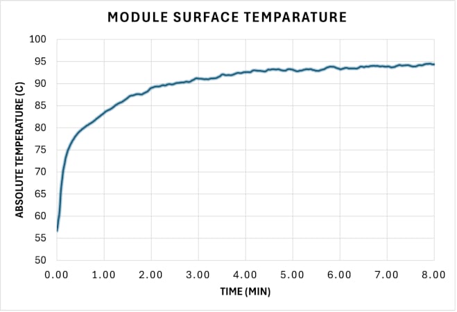
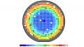
Figure 14. GT1 module temperature measurement. Image used courtesy of Bodo’s Power Systems [PDF]
Conclusions and Next Steps
Preliminary results have proved that embedding reduces the power loop parasitics resulting in “cleaner” switching waveforms and increased power density compared to a traditional “2D” design with surface discrete components. A next step will be building a new design iteration of the GT1 module which will include an embedded thermistor and current sensor. RAM has also designed and built a 650 V 60 A GaN module and plans to build 900 V GaN and 1200 V SiC versions.
This article originally appeared in Bodo’s Power Systems [PDF] magazine.