Facebook
 Google
 GitHub
 Linkedin
No Need for External Sensors in New Inverters
This article introduces IC integration to allow PCB based sensor solutions for the reduction of cost and footprint of power converters.
When it comes to trends in the power electronics sector, the rate of change is accelerating, with different emphasis being placed on key factors such as power density, performance or reliability depending on the final application. One requirement that remains constant however, irrespective of the application, is reducing costs. In fact, in any new development in the power electronics industry, from transistors to entire inverter solutions, cost savings are of the essence.
One of the main factors affecting costs and performance in converter technology is current sensing. The right solution is a compromise between cost and accuracy, or rather the dynamic characteristics of the measurement process. Many different current sensing techniques exist, with one of the best in terms of bandwidth and accuracy being fluxgate technologies. For cost reasons, these are usually limited to special niche applications. More common in the >100kW range are Hall-effect current sensors which, thanks to new integrated amplification circuits, deliver a high level of accuracy with integrated galvanic isolation. With new packaging technologies for power electronic systems, discrete solutions often tend to conflict with new overall system requirements. Active devices embedded in printed-circuit boards or PCB based AC and DC bus bars open up all sorts of new possibilities for integrating current sensing technology. The substantial market volume and the all-important costs factor have led to the development of a wider range of alternative current sensing methods. The market demand for isolated current sensors will hit the 100 million mark in 2020, which is roughly equivalent to the amount of iPhones produced in 2012.
How to find the right sensor solution for IGBT inverters
With the exception of some individual cases, current measurements are required within most applications, since the load current value serves as a basis for efficient control. The other need is related to providing the right protection under fault conditions. The decision over what current sensor technology to use does not only come down to dynamic characteristics and a reliable, interference-free function. In fact, accuracy and, of course, costs are also crucial to the decision. It goes without saying different applications have different requirements: in electric vehicles for example, the high RPM and large currents mean that bandwidths in the 100 kHz+ range are needed to deliver optimum results in terms of torque and motor efficiency. In other applications such as aviation, an error deviation of 0.5% across a temperature range of -50°C to 125°C is a must. In between is the majority of applications, made up predominantly of industrial, speed-controlled drives, voltage supply systems and regenerative energies. Another requirement is the scope of the insulating properties. Due to technical limits, not all current sensing techniques with reinforced insulation such as Hall-effect sensors can simply be replaced by shunts or IC solutions. In contrast, in the lower output range where basic isolation is sufficient, i.e. <80A and <400V, IC-based solutions are being used more and more frequently. This trend underlines the fact that sensor ICs are also increasingly being used in high-power applications thanks to the cost benefits they provide, and the generally easier integration of current sensing elements.
Current measurements are usually taken using auxiliary parameters: voltage in resistive current sensing methods and magnetic fields in magnetic methods. Other optical or mechanical methods are usually not economically viable in industrial applications today. Pure magnetic methods are based on the principle of the Hall effect, the B-field induces the Lorentz force on moving charge carriers and the magnetic fields of AC and DC currents are detected using Hall elements. Since both the charge carriers and the Hall voltages are dependent on temperature, the biggest challenge with Hall-effect sensors is ensuring that the accuracy requirements are met across the entire temperature range.
With open-loop sensors, the magnetic fields are shown directly as voltage without the signals having to be processed in any way. With this type of sensor, developments aim at improving signal amplification by using new ASIC technology. Open-loop sensors, which are unbeatable when it comes to size, weight and price, can already be found in many high-volume applications including eMobility.
If the magnetic flux in the magnetic core is balanced to zero, this secondary (compensating) current is the exact representation of the primary current. As a result, these closed-loop sensors deliver good overall accuracy across the entire temperature range.

Figure 1: An accurate closed-loop sensor in a SKiiP4 IPM with directly connected electronics
By integrating current sensors into the power module, they can be directly connected to the driver electronics and by noise resistance, transmitted to the controller unit. The measurement accuracy of the SKiiP4 IPM module integrated sensors is in the range of 0.5% across the entire temperature range with a bandwidth up to 100 kHz. Developments in the area of Hall elements centre on the improvement of the charge carrier mobility and, consequently, on greater accuracy. New materials such as indium antimonide (InSb) or graphene offer a way of doubling the mobility in the sensor element.
IC integration allows PCB based sensor solutions
New developments in power electronics work by eliminating costly materials and production processes. The use of a single, common carrier material from the power electronic chips to the controller chips might be one way to reduce costs in the future. PCB production involves reliable, automated processes, offering cost and time benefits in converter assembly. Challenges remain with regards to the reliability of different connection processes within, and to the PCB, as well as with regard to suitable cooling concepts. The clear advantages that this technology offers lie in the possibility of integrating control lines, reducing interference and parasitic effects. Semikron’s MiniSKiiP GB modules already offer a bus bar alternative for up to 250A and in the low power range, new developments for entirely PCB-based systems already exist, as do Hall-effect sensor ICs which can be directly assembled over the AC copper lines that are integrated into the PCB.

Figure 2: MiniSKiiP GB paves the way for SMD current sense resistors up to 200A
These modules allow for bandwidths up to 150 kHz and up to 0.7% accuracy, and existing sensing technology demonstrates verifiable linearity. The biggest challenge when using these solutions is the signal to noise ratio which is highly dependent on layout and converter design. Here, too, signal interference is caused by parasitic capacitance in the PCB traces and pads, just like in “large-scale” converter systems.

Figure 3: Impact of parasitic effects in the PCB on signal accuracy
A low-pass filter can help reduce noise, but cancels out any dynamic advantage this system has. Additional shielding can improve performance but reduces simplicity and cost benefits of the PCB based solution. So a well-proven PCB layout is a must for such a solution.
In addition to Hall-based current sensing ICs, there are also magnetic resistive methods like AMR sensors that are based on the anisotropic magnetic resistive effect, in which the resistance changes in relation to the external magnetic field. Here, the current measurement is identical to the closed-loop principle of differential magnetic field measurement with compensation. The current is fed through a U-shaped bus bar, creating a field gradient between the two sides of the bus bar. The sensor measures this difference and moves to zero by the compensation winding. The current which is required for the compensation determines the measurement signal.

Figure 4: New XMR sensor IC try to get rid of U shape) optional
The advantage of AMR technology is that the sensor exhibits no hysteresis and, thanks to the fast control loops incorporated in the IC, is suitable for bandwidths of up to 500 kHz, i.e. signals with rise times below 2µs. With the right PCB layout, this principle can cover a variety of current ranges. The main shortcoming of this solution remains accuracy, with the latest technology delivering approximately 2% accuracy. The challenge here is interference immunity with regard to external magnetic fields and the rather restricted sensor position possibilities, which makes PCB production especially challenging.
Besides these magnetic current sensing solutions, resistive current sensing is always a good choice due to the cost benefits it offers. Moreover, from technological advances in this area resistive current sensing is becoming increasingly viable for the >100A output ranges too. The basis of resistive current sensing involves measuring the induced voltage drop across the current-carrying conductor to infer the current. The challenges to be overcome here are the low voltage signal, which is in the millivolt range, the power dissipation at the moment the measurement is taking, as well as the need for separate galvanic isolation from the controller.
Nowadays, shunts that are used in challenging applications have to fulfil substantial requirements: 0.5% accuracy, resolution with 16 bits, high linearity and long-term stability up to 170°C, along with reinforced isolation. Integrating shunts into external bus bars outside of the power module is usually contrary to the aim to keep converters compact in size.
The alternative would be to integrate the shunt sensor into the power module directly. Up until now though, one of the main obstacles was the fact that costly IGBT chips potential needed to be used for the integrated shunt sensor. New shunt technologies and intelligent integration concepts open up new possibilities.

Figure 5: SEMIX Press-fit module with integrated shunts replaces external sensor solutions
Here, SEMIKRON’s solution is to replace existing contact bonds with shunt resistors, to efficiently integrate the current sensors into the power module without affecting power density. The module connection and module driving processes have to remain unchanged in order to ensure efficient system upgrades. SEMIKRON is the first in the industry to produce a standard 17mm module with integrated shunt resistors for up to 600A. The resistors used are based on an alloy that works unimpeded at temperatures of 250°C, and delivers very reliable results thanks to its ultra-low temperature coefficient. By incorporating the current sensing technology into the module, external sensors are no longer needed. Overall size and weight, two crucial factors when it comes to mobile applications are also lowered. The sensors are connected to driver electronics using press-fit connectors, requiring only a single step in the driver assembly process with no additional sensor mounting or connections. The high linearity of the shunts forms a reliable basis for challenging control tasks and the compact size of the shunts means they take up no additional space in the module, ensuring the module is identical to the standard version of the 17mm SEMiX 3 press-fit modules. The rated current is unaffected, i.e. none of the costly chip area is lost. There are also fewer interfaces thanks to the press-fit connection, resulting in better FIT (failure in time) rates in the final converter system. Likewise, separate pin connectors and their corresponding wires, as well as an addition sensor power supply are no longer required.
The use of integrated current sensors in power modules also brings about challenges: the voltage signal lies on DC link potential and has to be isolated and digitalised before it can be processed by the application controller. The module design has to work without restrictions in current symmetry and within the required temperature range. In addition to electrical specifications for shunts, including those for operation in threshold regions, e.g. losses under short circuit conditions, another aspect that has to be taken into account is the inductance of the shunt interconnection, bearing in mind that the shunts are integrated in the module. The voltage drop across this inductance during switching has to be as low as possible to prevent interference signals. Knowing these challenges, the new SEMIX pressfit with integrated shunts was successfully designed. The next challenge is to get the shunt signal without interference and in the right dynamic range and accuracy to the controller.
The isolation of the shunt signal can be optical, capacitive or inductive, although most sensor ICs that exist today use optical or capacitive coupling and the transmission can be realised using various protocols. One possibility is digitalise and transmit via a serial protocol like an UART that is later offered as differential interface to keep the noise robustness. Another possibility is to use delta sigma modulation to the controller requiring the addition of a clock signal. Knowing what system is more suitable depends on the given requirements for response, electric insulation capability, the interface definition for the controller solution and of course, costs.
Digital sensor signals lead the way
The UART based possibilities include the D/A conversion of the voltage signal on the secondary side and isolated transmission as a serial signal to the control unit. The dynamic response and the insulating properties have to be adapted to the given requirements. The main advantage of this solution is that it offers real galvanic isolation via transformers. For customers, this means separate isolation is not needed, especially in the >300A range. Another merit of this method is its high level of accuracy. In addition to the specified 0.5% error deviation of the shunts the accuracy is also subject to other A/D conversion and amplification stage tolerances. The performance characteristics with 6 Mbit/s that the controller can process directly, are sufficient to ensure efficient control. Plus, new controller families can process the serial protocol directly and a clock signal is not required.
Best performance with SEMIKRON evaluation Kit
Besides solutions with reinforced galvanic isolation in the higher voltage range, IC integrated couplers are also becoming increasingly important for shunt signal evaluation. The most common method used in the market is shunt signal conversion, using a sigma delta modulator with an isolation barrier in the IC itself.

Figure 6a: Sigma delta conversion IC ADS1203 with optical insulation

Figure 6b: Sigma delta conversion IC ADS1203 with capacitive insulation
In this process, it is only the difference that is integrated and transmitted with a 1bit signal over a single line. With oversampling of that signal the result can be optimized between accuracy and dynamics, depending on the application. If these solutions are used on the same circuit board as the main controller, there are no specific interference protection requirements. Using the same circuit board, the bit current can be fed directly to the controller which is delivering also the clock signal. If there is an interface between the controller board and the driver board, however, the low signal will mean that a signal transmission that is immune to interference has to be selected. Here, SEMIKRON works with a differential RS485 interface which allows the option of using wire-based controller connections so that system designs can be realised without from factor restrictions.
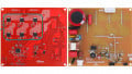
SEMIKRON offers a complete 3-phase application KIT based on the new SKYPER 12 and SEMIX press-fit shunt with fully integrated current sensing.

Figure 7: SEMIKRON Evaluation Kit without external current sensors
The new driver core SKYPER 12 is a galvanically isolated driver for SEMIX 3 press-fit modules featuring integrated shunt resistors. With an adjustable filter time, fast error management and an MTBF rate of 8 million hours, this driver delivers a reliable 2 watts and 20A peak output in a driver that’s smaller than the size of a matchbox. Thanks to the isolated voltage supply, the delta sigma IC draws its power on the secondary side of the SKYPER, meaning external isolation is not needed. SEMIX press-fit modules feature parallel shunts that are fed to the adapter board directly using press-fit pins, and thanks to the IC based sigma delta modulator, include galvanic isolation. The bit current is converted to an interference-free differential signal with a 20 MHz clock signal. This allows for direct digital signal filtering and resolution. The SEMIX modules are suitable for up to 600A and 1700V despite the integrated shunts. Thanks to the integrated NTC sensors and optional DC link measurement via auxiliary contacts, all the isolated signal conditioners can be integrated onto one PCB.
With this evaluation Kit of SKYPER 12 and SEMIX press-fit shunt, customers no longer need additional space for separate current sensors, a separate power supply, wiring or circuit board assemblies. One board now incorporates all of the isolated sensor signals. Depending on the alternatives, in the converter stack this can bring about savings of up to six percent. The use of integrated shunts in standard package 17mm modules therefore meet the all-important requirement to realise simple cost down projects in new converter solutions. Additionally, the direct connection covers the performance requirements of bandwidths of over 50 kHz and 1% accuracy. With the evaluation kit, the system can also be adjusted to meet the requirements of the given application in absolute minimal time. Plus, thanks to the press-fit architecture, the entire electronics are mounted in one single step. The converter has a single interface and does not require separate signal conditioning boards, making it an optimum low-cost current sensing solution for use in future developments.
About the Author
Johannes Krapp studied industrial engineering at the University of Applied Sciences Würzburg-Schweinfurt. As senior product manager he is responsible for driver electronics and stack assemblies at SEMIKRON.
This article originally appeared in the Bodo’s Power Systems magazine.