Facebook
 Google
 GitHub
 Linkedin
New 800A1200V Full SiC Module
This article describes Mitsubishi Electric's new 800A/1200V full SiC module and its advantages over conventional IGBT modules in power electronic systems.
The evolution of SiC technology in power modules and its principle loss reduction potential are shown in Figure 1. Mitsubishi has developed two new full SiC module types with 800A and 1200A rated currents and 1200V rated voltage [1]; [2]. This article is describing the 800A module.

Figure 1: Evolution of SiC technology in power modules
Package outline and circuit diagram
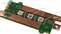
The appearance of new 800A/1200V full SiC module (type name: FMF800DX-24A) and its internal circuit diagram are shown in Figure 2. The module contains 2 x 400A half-bridge configurations. By externally paralleling the main P-, N- and AC-terminals an 800A/1200V 2in1 configuration is formed. By this paralleling approach, the internal package inductance LS has been decreased to less than 10nH, which is important for limiting the overvoltage spikes at chip-level due to high di/dt at switching of SiC-MOSFET.

Figure 2: FMF800DX-24A package outline and internal circuit
The baseplate dimension of FMF800DX-24A is 62mm x 121mm. Thus the module size of new 800A/1200V full SiC module is about 1/2 compared with conventional Si-based IGBT modules having the same current rating, see Figure 3.

Figure 3: Footprint comparison
For monitoring the baseplate temperature TC an NTC-sensor located close to the MOSFET/FWDi chips is incorporated into the module. For short circuit and overcurrent protection MOSFET-chips with on-chip current sensing are used in one of the half-bridge configurations (see Figure 2).
Main module parameters
The main parameters of 800A full SiC module are shown in Table 1. The values of VDS, RDS(on) and VSD are given on chip level.

Table 1: Main FMF800DX-24A parameters
Switching characteristics
Typical turn-on and turn-off switching waveforms at VCC=800V; TJ=150°C; RG(on)=RG(off)=5Ω are shown in Figure 4 and 5 for different drain currents ID=140A…1400A.

Figure 4: Turn-on waveforms

Figure 5: Turn-off waveforms
For limiting the turn-off overvoltage spike a cross-snubber capacitor of CS=6µF was connected between P- an N-terminals. The dependency of switching speed di/dt on drain current ID is shown in Figure 6 and 7 for different junction temperatures TJ=25°C; 75°C; 125°C; 150°C and different DC-link voltages VCC=600V; 800V.

Figure 6: Turn-on di/dt versus ID

Figure 7: Turn-off di/dt versus ID
Two comments can be derived from Figure 6 and 7:
- The current slopes at turn-on and turn-off don’t show a strong dependency on-chip temperature TJ and DC-link voltage VCC. This behavior differs from today’s IGBT-modules.
- The maximum di/dt at turning-off ID=1400A was about 13A/ns, which is quite similar to the switching speed known from today’s high current 1200V IGBT-modules.
Loss comparison with Si-based IGBT modules
The typical forward characteristics of new 800A full SiC module and existing 800A Si-based IGBT module are compared in Figure 8.


Figure 8: Forward characteristics
The comparison of switching energies in Figure 9 is indicating a key benefit of SiC technology: the switching losses can be drastically reduced compared with Si-based IGBT modules.


Figure 9: Switching energy comparison
This benefit can be seen in the power loss simulation results per Transistor/FWDi-pair in inverter operation for two different PWM frequencies 15kHz and 30kHz and the corresponding temperature rise ΔT(j-c) in Figure 10 and Figure 11.
The total power loss can be drastically reduced (by 71% for 15kHz and 76% for 30kHz ) when full SiC-module is used. This loss reduction is mainly due to reduced switching loss. Conclusion: full SiC modules are very well suited for applications requiring high switching frequencies, where conventional Si-IGBT modules are reaching their thermal limit.

Figure 10: Loss and ΔT(j-c) simulation at fc=15kHz; VCC=600V; IO=400A(peak); PF=0,8; M=1,0

Figure 11: Loss and ΔT(j-c) simulation at fc=30kHz; VCC=600V; IO=400A(peak); PF=0,8; M=1,0
Gate Driver with SC-protection
The new 800A/1200V full SiC-Module can withstand a short circuit current for a limited time of tSC(max)=2,5µs. This limit is given in the SCSOA specification.
For conventional Si-IGBT modules typically a short circuit capability of tSC(max)=10µs is specified. In such conventional IGBT drivers, a blanking time between desat-detection and SC-turn-off of typically to=1 3µs is installed, which is sufficient to ensure both: no false SC protection tripping and safe SC-turn-off.
Considering the relatively short tSC(max)=2,5µs specified for the new 800A/1200V full SiC-module another SC-protection method is proposed, known as RTC (Real Time Current Control). For this purpose one p-side and one n-side SiC MOSFET chip are equipped with a current sense electrode (refer to Figure 2). The equivalent circuit and the external view of this SiC MOSFET chip are shown in Figure 12.


Figure 12: SiC MOSFET chip with current sense terminal
The functional block diagram of a dedicated gate driver for FMF800DX-24A using the proposed RTC protection is given in Figure 13. The measured short circuit waveforms during RTC operation are shown in Figure 14.


Figure 13: Principle of SC-protection by RTC

Figure 14: SC-waveforms during RTC-operation
During SC-turn-off operation by RTC four modes can be distinguished. In mode, the main current ID is increasing until the voltage Vs across the shunt resistance is reaching a defined trip level. After reaching this trip level the mode starts: the transistor T is turned on and the Gate-Source voltage is reduced from +15V to about +7V resulting in a decreased SC-saturation current. Due to this SC-current reduction, the allowable short circuit time is increased again to the well-known from IGBT drivers tSC(max)=10µs. Means from now on the conventional IGBT gate driver timing can be applied. During phase, the gate driver transistor Tron is switched off and VGS becomes Zero thus causing a soft turn-off of the short circuit current. In the final phase, the driver transistor Troff is turned on thus applying a negative VGS to the SiC MOSFET in off-state.
Summary and outlook
This paper is describing a new 800A/1200V full SiC dual module. Its type name is FMF800DX-24A. Compared with conventional Si-based IGBT modules the following unique points are confirmed:
- Module size reduced by 50%
- Switching loss (Esw= Eon + Eoff + Err) reduced by 75%
- Reliable SC-protection by RTC
Based on these features the new 800A/1200V full SiC module provides an interesting alternative to conventional IGBT modules in power electronic systems up to several 100kW, especially if one of the following system characteristics is of specific importance:
- Compact equipment size/high power density
- High efficiency
- High switching frequency (beyond the today’s limit reachable with IGBT modules)
About the Authors
Eckhard Thal graduated from the Moscow Power Engineering Institute in 1980. Same year he joined ELPRO Berlin as a design engineer in the inverter development. In 1991 he received his PhD in the field of power electronics at the Chemnitz University. Since 1991 he is working for Mitsubishi Electric Europe (Ratingen/Germany) in application engineering for power semiconductors.
Koichi Masuda worked at Mitsubishi Electric that operates on the corporate principle of contributing to creating a vibrant and affluent society by enhancing its technologies, services, and creative powers, as a leader in the manufacture and sales of electric and electronic equipment used in Energy and Electric Systems, Industrial Automation, Information and Communication Systems, Electronic Devices, and Home Appliances.
Eugen Wiesner is an Application Engineer at Mitsubishi Electric Europe B.V., Ratingen Germany, one of the branches of the Japanese multinational electronics and electrical equipment company, Mitsubishi Electric Corporation. the company manufactures electrical and architectural equipment and is one of the major producers of photovoltaic panels.
References
- Press release No.2687 “Mitsubishi Electric to begin shipment of Silicon Carbide Power Modules Samples”, Tokyo, July 9, 2012
- Press release No.2733 “Mitsubishi Electric develops Large capacity SiC Power Module Technologies” Tokyo, February 14, 2013