Facebook
 Google
 GitHub
 Linkedin
Sensor Placement Errors in High-Voltage Systems That Distort Measurements
Improper sensor placement in high-voltage systems can lead to distorted measurements. This article explains how ground shifts, dv/dt, and layout mistakes can affect your results.
Earlier articles covered probe loading and oscilloscope bandwidth, showing how probe capacitance affects fast edges and how limited bandwidth can quietly hide critical harmonics. Fixing these issues helps you get a clean, accurate waveform. Still, even with a well-compensated probe and plenty of bandwidth, high-voltage measurements can be inaccurate. This is because the measurement location in a real high-voltage system is almost never electrically neutral, which is why datasheets rarely mention it.
In theory, a node is just a point, but in real hardware, it is a physical area with its own resistance, capacitance, inductance, and electromagnetic effects. Ground is not always at the same potential everywhere, and a switching node does not have just one voltage. The current path is not a straight line either. It is a network of impedance spread through copper, air, and dielectric materials.
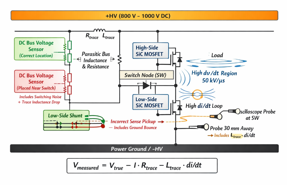
Figure 1. Sensor placement effects in high-voltage SiC half-bridge. Parasitic bus resistance and inductance, combined with high dv/dt and di/dt switching transients, cause measurement voltage to deviate from the true bus value depending on sensor location. Image used courtesy of Bob Odhiambo. (Click on image to enlarge).
In high-voltage, high-power systems like 600 V inverters, 1 kV DC links, or SiC half-bridges switching at 50 kV/µs, spatial effects are no longer minor, they become the main source of measurement errors. Where you place a sensor in the circuit can cause problems such as parasitic impedance between the node and the measurement point, magnetic coupling, ground shifts, capacitance pickup, and thermal gradients that affect resistive sensors.
This article looks beyond measurement instruments to show how sensor placement in high-voltage systems can quietly change current and voltage readings. It also explains why 'ground' is often unstable and how layout choices can cause errors big enough to affect your design decisions.
High dv/dt and di/dt Danger Zones
When sensor placement is an overlooked factor, high dv/dt regions are where problems often happen. In high-voltage power systems, not all nodes are the same. Some are on stable DC rails, while others act like strong electromagnetic sources. The most problematic areas include the switching node of the half bridge, the gate drive loop, the return path of the current shunt, and the motor’s phase output.
In a 600 V half-bridge, the switching node moves from 0 V to 600 V in just a few nanoseconds, at a rate of 50 kV/µs. Now, think about a small stray capacitance of only 2 pF between the switching node and a nearby sensor trace. We can use the relationship between capacitance, current, and voltage rate of change here.
$$I = C \frac{dv}{dt} = (2 \times 10^{-12})(50 \times 10^3) = 100 \text{ mA}$$
The resulting 100 mA of displacement current does not just disappear; it has to go somewhere. In this case, it often flows into nearby conductors, including your sense line. If the sense line has as little as 10 ohms of impedance at high frequency, the outcome is clear:
$$V = I \times Z = 0.1 \times 10 = 100 \text{ V spike}$$
This causes a one-volt error almost instantly, not because of limited scope bandwidth or a bad probe, but because electric field coupling goes straight into the measurement path.
For gate drive loops, the average gate current is important, but the peak current during a nanosecond transition can reach several amps. Consider the effects of just 10 nH of stray inductance with a 5 A current switching in 20 ns. That is a di/dt of 250 A/µs. The resulting voltage is:
$$V = L \frac{di}{dt} = (10 \times 10^{-9})(250 \times 10^6) = 2.5 \text{ V}$$
This voltage appears locally across the loop. If your measurement ground shares any part of the return path, you have just introduced a 2 to 3 V error into what you thought was a clean gate signal. This often leads engineers to misinterpret false Miller turn-on or phantom ringing.
Thermal Gradients and Sensor Bias Errors
Instead of sudden voltage spikes, thermal gradients cause gradual drifts that can be mistaken for real system behavior. Shunt resistor self-heating during power use follows this relationship:
$$P = I^2R$$
For example, a 5 mΩ shunt carrying 40 A will dissipate 8 W of power, as shown below. For a small metal component, this amount of power is not negligible. As the element heats up, its resistance changes in proportion to the temperature shift. This affects the final reading and is shown as:
$$R(T) = R_0 (1 + \propto \Delta T)$$
Where you place the thermocouple and the Hall sensor also greatly affects how accurately they measure. If a thermocouple is placed on a heatsink, in airflow, or away from the real heat source, it will report inaccurate values. Hall sensors are also sensitive to temperature, so mounting them near hot components can shift their offset and gain, adding a DC bias to the current measurement.
With layout and airflow, uneven heating across a PCB can unbalance differential traces and amplifiers, turning small resistance changes into measurement errors. In high-voltage systems, where you place these sensors affects both electrical and thermal exposure. This can distort readings as much as electrical noise, so correct placement is crucial.
PCB Layout-Induced Measurement Errors
A poorly designed PCB layout can corrupt measurements before the signal even leaves the board. In high-voltage, high dv/dt systems, layout is more than just aesthetics; it affects the electromagnetic environment your sensors must work in. One common PCB design mistake is routing the sense trace next to high-current loops. For example, a current shunt in the power return path may have thin sense lines that run parallel to a switching node or high-current copper area.
When a high current loop, such as 30-50 A, switches in tens of nanoseconds, it generates strong magnetic fields. If the sense traces run alongside, they become part of a coupled loop, adding voltage directly into the measurement. Even if the induced voltage is only tens of millivolts, that is significant when the shunt signal spans just 100 mV, enough to distort or hide the true signal.
Another critical layout flaw is incorrect differential routing, where positive and negative sense traces are routed over different reference planes. For example, the positive trace might cross a noisy power ground, while the negative runs over a clean ground. This creates asymmetry, so each trace faces different parasitic capacitance and return path impedance. As a result, common-mode noise can turn into differential error. Even though the amplifier is differential, engineers often assume it is immune, but in reality, the measurement is compromised.
Design Rule for Correct Sensor Placement
As discussed in this article, the integrity of measurement in high voltage systems is not just about one mistake. The table below summarizes the most critical design considerations and the problem each rule prevents.
| Consideration | What To Do | Importance | Consequence If Ignored |
| Minimize Loop Area | Route sense traces tightly coupled and parallel; avoid large current loop proximity | Reduces magnetic coupling from high di/dt paths | Induced voltage spikes and switching-synchronous noise |
| Use True Kelvin Connections | Take sense leads directly from the shunt element, not shared copper | Eliminates voltage drop from trace resistance and ground bounce | Inflated or distorted current measurements |
| Reference the Correct Ground Domain | Ensure measurement reference matches the intended return path | Prevents hidden ground lift and domain mismatch | Clean-looking but misleading waveforms |
| Avoid High dv/dt Regions | Keep sense traces away from switching nodes and phase outputs | Minimizes capacitive displacement current injection | Edge-correlated voltage spikes |
| Control Thermal Exposure | Avoid hotspots and airflow asymmetry; consider the temperature coefficient | Limits resistance drift and sensor bias | Slow systematic measurement drift |
| Validate Physically, Not Just Electrically | Compare multiple pickup points and measure ground-to-ground voltage | Detects spatial and reference-induced errors | Undetected layout-induced distortion |
Table 1. Core design considerations for accurate sensor placement in high voltage systems.
The six considerations outlined in the table above are aimed at protecting voltage measurement from spatial distortion. However, there is another quantity even more sensitive to placement error and often misinterpreted in high-voltage systems: common-mode current.
Unlike differential current, common mode current is not restricted to a single return path. Instead, it spreads through parasitic capacitance, chassis connections, motor cables, and protective earth. Poor sensor placement can either amplify or completely hide it. In fact, the layout mistake discussed in this article directly impacts how common-mode current appears in a measurement.
In the next article, we will go beyond placement fundamentals and explore practical methods for measuring common-mode current accurately in high dv/dt, high voltage environments. In these cases, the choice of reference, sensor geometry, and bandwidth discipline becomes even more important.
Related Content