Facebook
 Google
 GitHub
 Linkedin
Mitigating DC Link Anti-Resonance for WBG-Based Designs
What causes failure in wide bandgap semiconductors, and how can engineers mitigate them?
This article is published by EEPower as part of an exclusive digital content partnership with Bodo’s Power Systems.
A basic requirement for DC link capacitors is the maximum ripple current they must carry. However, even with correct component selection for this rating, parts of the capacitor bank can become much hotter than calculated, especially in fast-switching converters with wide bandgap (WBG) semiconductors, leading to catastrophic failure in some cases. Responsible for this are hidden currents due to parasitic resonance.
By using silicon carbide (SiC) devices, AC-DC and DC-DC converters are rapidly evolving into systems with higher switching frequencies, efficiencies, and power densities. Because the voltage (du/dt) and current (di/dt) transients are more than ten times faster than in silicon devices, parasitic component effects become much more critical. As a result, the voltage overshoot is higher and ringing lasts longer. This can affect the service life of active and passive components.
A key functional block inside a typical converter is the DC link and all associated components. It often performs the following three functions:
- Providing energy storage capability for averaging the rectified mains voltage (grid frequency -50/60 Hz)
- Handling the switching frequency (plus harmonics) ripple current caused by the switching devices (typical switching frequency -20 kHz to 150 kHz range)
- Providing a sufficiently low high-frequency commutation loop inductance to avoid an excessive voltage overshoot when high di/dt values are applied during switching (MHz range)
The first two functions are often accomplished by the same capacitors in terms of technology. For the last function, an additional low-inductance component is often required, which typically has a low capacitance and must be placed next to the power semiconductors. Especially for converters with wide bandgap semiconductors, these become increasingly important due to the high di/dt values.
Usually, one capacitor technology handles the low-frequency part (LF) and thus the first two tasks and is named CLF in the following. The other is for the high-frequency portion (HF) and is called CHF. Since CLF is much higher in capacitance than CHF and, therefore, mechanically much larger, long interconnection structures are usually involved in between. This results in this equivalent circuit diagram (Figure 1).
Although a laminated busbar, for example, can minimize the parasitic inductance of the interconnect structure (Lparasitic), this must always be carefully considered when analyzing the capacitive function block of the whole converter.
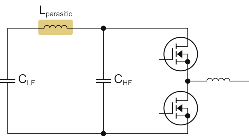
Figure 1. Equivalent circuit of the commutation loop with the parasitic inductance of the interconnection structure Lparasitic. Image used courtesy of Bodo’s Power Systems [PDF]
Simplified Equivalent Circuit
Certain aspects can be simplified to better understand the mechanism of anti-resonance.
Taking the parallel configuration of the LF and HF capacitors as a starting point, the interconnection structure has a certain parasitic inductance (Lparasitic; Figure 2a). Since the frequency range of interest is usually above the (series) self-resonant frequency of the LF capacitors, it can be substituted by the ESL only without considering the capacitive component (see Figure 2b). On the other hand, the frequency range considered is usually well below the self-resonant frequency of the HF capacitors, so they can be approximated by their capacitive part only without considering the ESL. Finally, the ESL of the LF capacitors and the parasitic L value of the interconnect structure can be summed to a single inductance, resulting in the simple LC parallel resonant circuit shown in Figure 2c. This will approximate the response of the entire circuit of LF and HF capacitors in the frequency domain of its impedance peak. This parallel resonant tank phenomenon is known as anti-resonance.
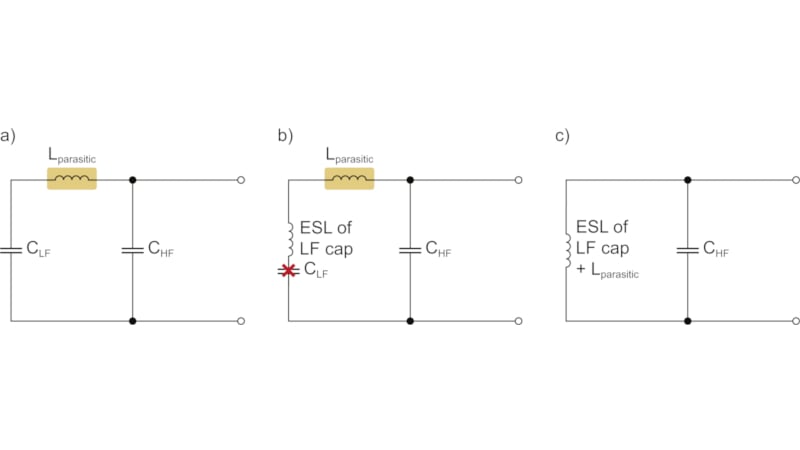
Figure 2. Equivalent circuits: a) LF and HF capacitor portions in parallel with parasitic L of the interconnection structure. b) LF capacitor in detail (i.e., C and ESL in series) with C being neglected. c) Resulting simplified equivalent circuit at anti-resonance frequency; ESL and parasitic L summed up. Image used courtesy of Bodo’s Power Systems [PDF]
For this simplified equivalent circuit, the resonant frequency can be determined as follows:
\[f_{res}=\frac{1}{2\pi\cdot\sqrt{(ESL_{LF}+L_{parasitic})\cdot C_{HF}}}\]
At this anti-resonance frequency, the impedance of the circuit rises (significantly) above the expected value compared to when the impedance of the individual elements is considered separately.
For simplicity, the equivalent series resistances (ESR) of the components were not considered in the following analysis. In general, however, a higher ESR means a lower quality factor of the resonant circuit, so the resonance is wider and flatter, and vice versa.
At this stage, it is most important to understand that three crucial reactive elements determine the anti-resonance frequency:
- the resulting ESL of the LF capacitor bank,
- the inductance of the interconnection structure between the HF and LF capacitors, and
- the capacitance of the HF capacitors.
Calculation Examples
Two examples – one not optimized and one optimized – will be simulated using the simplified equivalent circuit diagrams (Figures 3 through 5). Subsequently, the optimized example will also be measured in a real system. In the simulation, the impedance measurement occurs at the point where the semiconductor switches are connected in the real system (I1 is used here for the impedance measurement).
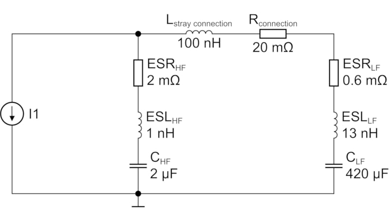
Figure 3. Equivalent circuit diagram of the highly inductive DC-link circuit. Image used courtesy of Bodo’s Power Systems [PDF]
In the first, not optimized example (Figure 3), three LF capacitors of 140 µF each (total CLF = 420 µF) are connected in parallel, each having an ESLLF of 40 nH (total approx. 13 nH) and an ESRLF of 0.6 mΩ. In this case, the busbar is poorly designed, resulting in a total inductance (Lstray_connection) of 100 nH. At the same time, some may be concerned about having enough HF capacitors, so a total of 2 µF is used as CHF. The frequency curve in Figure 4 shows an impedance peak at about 330 kHz that cannot be explained only by the individual capacitors' impedance curves. This peak is the so-called anti-resonance of the overall circuit.
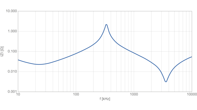
Figure 4. Frequency curve for the highly inductive DC-link circuit. Image used courtesy of Bodo’s Power Systems [PDF]
For example, if a resonant converter is attached to such a design and operated at about 110 kHz, which is not a big challenge for resonant SiC topologies, the strong third harmonic of the ripple current at 330 kHz would fully hit the impedance peak of this poorly designed DC link. In this case, resonant currents are likely to circulate between the capacitors CHF and CLF, and the parasitic inductances (Figure 3) are much higher than the harmonic of the ripple current itself. This can cause the capacitors to overheat and even fail, as this resonant current causes additional losses at the ESR (I2·R).
This example illustrates how harmful anti-resonance can become and how important it is to ensure a proper RF design, even in the so-called low-frequency portion of such mixed DC link capacitor assemblies.
In the second optimized example (Figure 5), the LF capacitors are exactly the same as in the first, but close attention was paid to a low-inductance design. The busbar has a leakage inductance of 20 nH and an ESR of 25 mΩ. The HF capacitor bank has a total of 1 µF (CHF), an ESLHF of 2 nH, and an ESRHF of 4 mΩ.
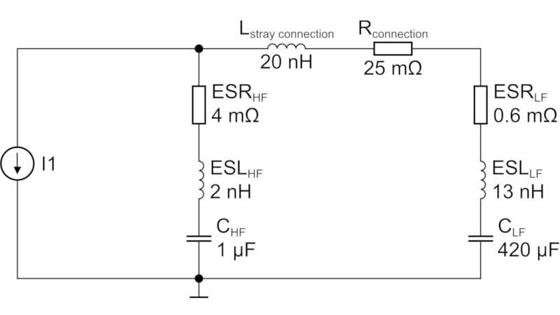
Figure 5. Equivalent circuit diagram of the low-inductance DC link. Image used courtesy of Bodo’s Power Systems [PDF]
In Figure 6, the impedance peak is located at about 850 kHz, a much higher frequency than in the first example.
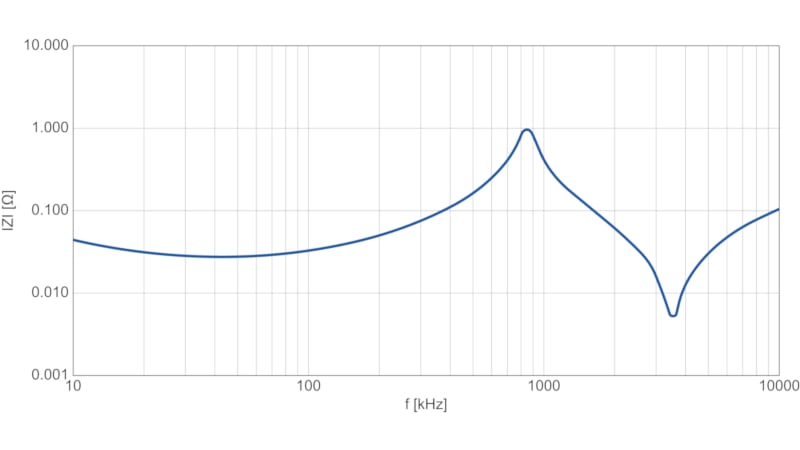
Figure 6. Frequency curve for the low-inductance DC link. Image used courtesy of Bodo’s Power Systems [PDF]
Mitigating the Anti-Resonance Effect
Based on the three critical factors that determine the anti-resonance frequency, there are strategies for dealing with the issues caused by anti-resonance:
- Shift the anti-resonance frequency to higher frequencies. This can be achieved primarily by reducing the ESL of the LF capacitors and any parasitic inductance in the interconnect structure. Keep in mind that the lower capacitance values of the HF capacitors or snubbers can also contribute to this. The goal of this strategy is to ensure that the anti-resonance is not hit by the ripple current or by low-order harmonics with their higher power levels.
- Move the anti-resonance frequency below the switching frequency. The objective of this strategy is also to ensure that the anti-resonance is not stimulated by the ripple current. An additional choke is often inserted between the LF and HF capacitors to move the anti-resonance frequency this far. This increases the inductance of the interconnect structure significantly. Additionally, it may also be useful to massively increase the capacitance of the HF capacitors.
- Set all switching frequencies of the system and their harmonics outside the critical anti-resonance frequency band. Attention must be paid to the tolerances and aging behavior of the passive components in the DC link as their values may vary and thus directly affect the anti-resonance frequency. Sometimes this strategy proves impossible, for example, when the switching frequencies vary over a wide range during operation, such as in resonant topologies.
- Selective attenuation of the anti-resonance impedance peak. This theoretical option adds a resistive element to the circuit that is effective only in the relevant frequency range and does not unduly affect the regular ripple current. Such a mechanism could, for example, use the skin effect in the interconnect structure since its resistance increases with frequency. This strategy could be promising in combination with the first strategy mentioned above. Further research is still needed to prove it and provide practical design guidance.
Remember, the ESR of aluminum electrolytic capacitors usually decreases significantly with temperature. Therefore, a converter that works perfectly at +25 °C may exhibit anti-resonance at higher temperatures.
Double Pulse Test as Metrological Verification
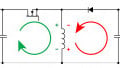
With a double pulse test, the anti-resonance oscillation can also be determined directly from the voltage waveform. Figure 7 shows the equivalent circuit of the double pulse test of a CHF/CLF structure with the parasitic elements. These include the ESLs of CLF and CHF, the inductance of the interconnect structure (Lparasitic), the parasitic inductance of the busbar or PCB between CHF and the devices (Lstray connection), the parasitic inductances of the drain and source terminals of the devices (LD, LS), the parasitic capacitance of a freewheeling diode (CDD), the equivalent parallel capacitance of the inductive load (CEPC), and the parasitic inductance of the meter (Lsense). The gate loop includes the parasitic inductance of the gate (LG) and the source terminal (LS). Also, the parasitic capacitances in the MOSFETs (CGD, CGS, and CDS) must be considered.
It is particularly important to note that the measurement continues after the second pulse has been turned off. Here, both components are off, but the body diode of the upper switch is still conducting, driven by the coil current (green arrow in Figure 7). Therefore, the DC link voltage (plus the nearly constant voltage drop of the body diode) is also visible at the switching node during this time. This means that voltage oscillations, especially between CHF and CLF, can be easily detected at the switching node even in this operating state. In the case of an anti-resonance oscillation, high currents flow back and forth between CHF and CLF (red arrows in Figure 7).
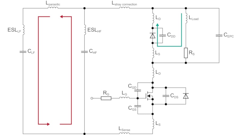
Figure 7. Equivalent circuit diagram of a double-pulse test setup with parasitic elements as well as the free-wheeling current (green arrow) and the anti-resonance current (red arrows). Image used courtesy of Bodo’s Power Systems [PDF]
Although CHF has a low impedance at the typical anti-resonance frequencies, the large oscillating currents can cause voltage oscillations across this capacitor, which can be observed at the switching node (Figure 8).
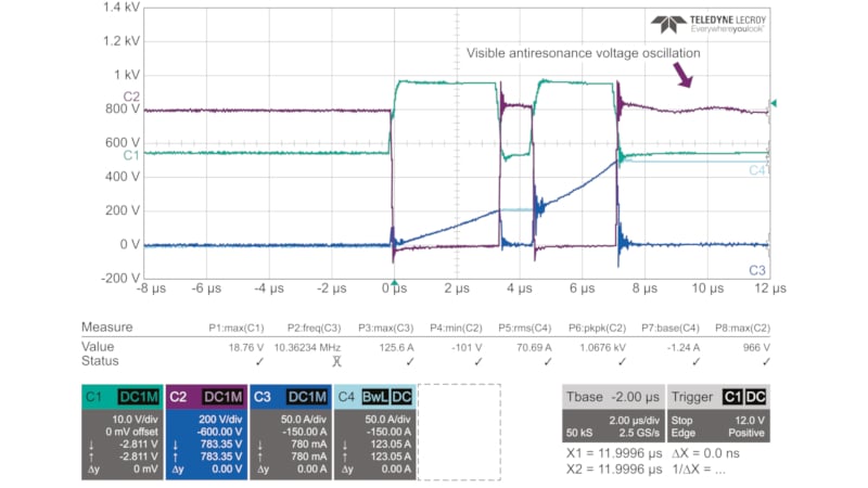
Figure 8. FF8MR12W2M1P_B11 double pulse test with the unoptimized example; in violet, the voltage at the switching node oscillates with an anti-resonance frequency around 400 kHz. Image used courtesy of Bodo’s Power Systems [PDF]
Results With a 50 kW EV Charger Test Setup
Figure 9 shows the power conversion board of a 50 kW EV charger test setup where the anti-resonance issue was solved. For this purpose, the busbar (Lparasitic) was optimized with the CHF values to reduce the oscillating currents in the loop. Multiple parallel terminals of the busbars help to reduce the effective inductance (Lparasitic) in the path. Knowing the natural resonant frequency of this resonant circuit helps the designer select the proper switching frequency of the converter. Stimulating the natural resonant frequency by harmonics of the switching frequency should be avoided.
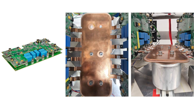
Figure 9. On-board CHF and multi-terminal busbar on an Infineon power conversion board for DC EV chargers. Image used courtesy of Bodo’s Power Systems [PDF]
The oscillogram (Figure 10) shows a waveform example after design optimization. The voltage at the switching node is the light blue curve and shows an anti-resonance oscillation with a frequency of about 1 MHz over a time of some 1 μs.
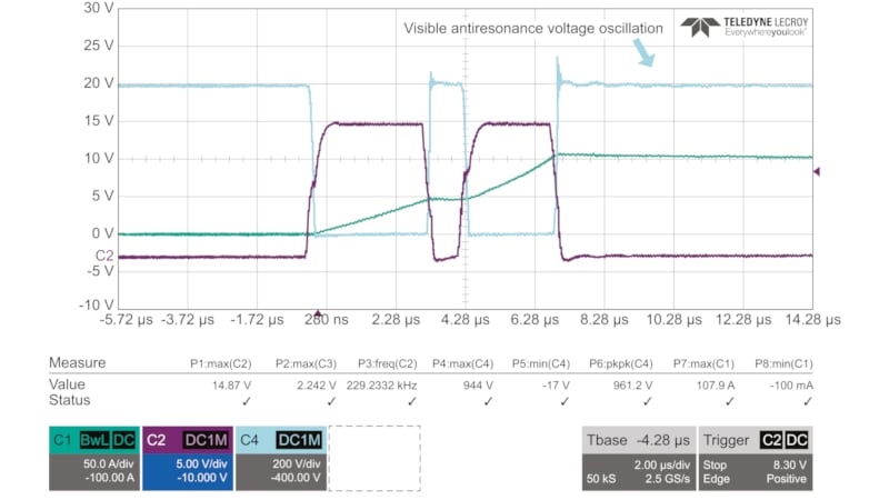
Figure 10. FF8MR12W2M1P_B11 double pulse test with the optimized 50 kW power converter test setup by Infineon. Image used courtesy of Bodo’s Power Systems [PDF]
Takeaways
Power system designers should thoroughly investigate anti-resonance issues early in the development process to avoid serious, unanticipated degradation of power converters in later design phases and even failures during operation. Choosing the right switching speed and frequency for the power converter, properly designing the commutation loop, including the busbar, and properly selecting the reactive components, such as the HF and LF capacitors, appropriately can mitigate a catastrophe before it happens.
This article originally appeared in Bodo’s Power Systems [PDF] magazine and is co-authored by Martin Neudecker, Manager of Industry Segment Development, TDK Electronics, and Pradip Chatterjee, Principal Engineer, Infineon.