Facebook
 Google
 GitHub
 Linkedin
DC/DC Converters: Devices for Supplying Negative Voltage
Read on to learn more about the basics of inverting converters and how they work.
Switch-mode power converters have been used profusely in modern electronics technology across multiple sectors, including industrial, commercial, utility, and consumer markets for several years. For low-power DC/DC conversion-based applications, most modern power conversion is accomplished using three major types of power converters – buck, boost, and buck-boost. However, some specific electronic circuits require power sources with the negative voltage at the output side. The inverting switching converter is a DC/DC converter type that enables the supply of negative voltage. Most basic DC/DC converter topologies can be modified to function as inverting converters.
Basics of Inverting Converters
The main intention of an inverting converter is to provide a negative voltage at the output. Besides this functionality, polarity inverting topology is extremely useful to power loads independent of polarity in reference to a system ground but supplied by an input voltage that may be either higher or lower than the output voltage [1]. The inverting topology typically uses a single inductor and does not require any coupling capacitor [2]. This leads to using fewer components to implement an inverting topology. However, because of the narrow range of applications to which it caters, it is employed less often than the other basic DC/DC converter topologies. For the scenarios which deal with larger rectifier currents, either a synchronous buck or a synchronous boost device is employed [3]. This helps in improving efficiency by reducing the conducted losses.
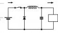
The implementation of an inverting converter can be accomplished in many ways. It could be by negative referencing, that is, turning a positive voltage to a negative voltage using any buck device. It could also be by positive referencing, turning a negative voltage into a positive voltage by utilizing any boost device [4]. One of the specific types of inverting converter topologies is an inverting buck-boost converter. Figure 1 illustrates the buck topology, boost topology, and the polarity inverting buck-boost topology. It is known to be a simple and low-cost polarity inverting converter with few power stage components. It has the advantages of a low component count and less development complexity, and its implementation can be done using a standard high-side regulator integrated chip. These are the ones intended for buck converters as well.
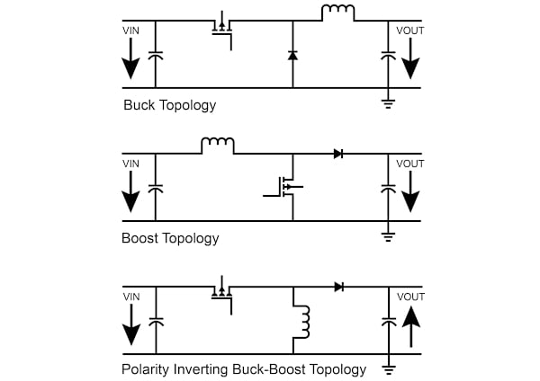
Figure 1. Circuit diagram of buck topology, boost topology, and a polarity inverting buck-boost switching converter. Image property of EETech
It is known to invert the orientation of the input voltage by utilizing a true flyback topology and is similar to the conventional flyback converter topology as it has a winding ratio of 1:1. The current is pulsed both at the input and at the output. Since the output voltage flies back to the switch node, it is referred to as flyback voltage, and thus, the voltage stress across the semiconductor-based switch is the sum of both input and output voltages. The controller is referenced to either negative input or output; thus, it must withstand the sum of input and output voltages.
High-level Buck-boost Converter Operating Principle
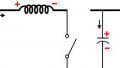
The polarity inverting buck-boost converter is a basic power conversion topology. It is implemented using an active switch (usually a MOSFET), a passive switch (typically, a diode), and an inductor [1].
Figure 2 illustrates the working of an inverting buck-boost converter. When the switch is conducting (referred to as on time), the input voltage is present across the inductor forcing a current to the ground. The energy is stored in the air gap in this case. When the diode is conducting, and the switch is off (referred to as off time), the inductor voltage flips and leads to the conduction of the rectifier. This leads to a negative voltage at the output. The current flowing during the on time is usually referred to as magnetizing current, whereas the current flowing during the off time is called the flyback current. The energy stored in the inductor during the on time is used to drive the flyback current [5].

Figure 2. Circuit diagram illustrating the working of an inverting buck-boost converter. Image property of EETech
The transfer function for this topology can be represented as
\[V_{out} = -V_{in}. (T_{on}/T_{off})\]
The ratio of on-time to off-time is referred to as the duty cycle and is represented by D.
Key Take-aways
- The inverting switching converter is a type of DC/DC converter that enables the supply of negative voltage.
- The inverting topology typically uses a single inductor and does not require any coupling capacitor.
- Polarity inverting buck-boost converter is a simple and low-cost polarity inverting converter with very few power stage components.
- The transfer function for an inverting buck-boost converter can be represented as Vout = -Vin. (Ton/Toff).
Key References
1. Buck-boost topology delivers negative output from positive input
3. Differences Between the Ćuk Converter and the Inverting Charge Pump Converter
4. Rudolf P. Severns and Gordon E.Bloom, Modern DC-to-DC switch-mode power converter circuits, 1985
5. Topology Tutorial: What is an Inverting Buck-Boost?