Facebook
 Google
 GitHub
 Linkedin
Level Shifting Challenges in Inverting Buck-Boost Circuits
Working with a switching regulator IC with an inverting buck-boost circuit can be a balancing act, and adequate level shifting is essential. This article provides a smarter approach to inverting buck-boost circuits.
This article is published by EEPower as part of an exclusive digital content partnership with Bodo’s Power Systems.
The magnitude of the negative voltage generated by inverting buck-boost circuits can be higher or lower than the available positive voltage. For example, –8 V or even –14 V can be generated from +12 V. When working with a switching regulator IC with an inverting buck-boost circuit, the system design may need communications pins. If they do, designers must remember adequate level shifting so synchronization and enable signals can be utilized.
Why Is Level Shifting Required?
Inverting buck-boost circuits are commonly used to generate negative supply voltages from positive voltages. The most important step is ensuring the negative voltages are generated correctly. However, additional level shifting circuits may be necessary if the main application circuit controls or supervises the power supply. It has a reference to ground, while the GND pin of the inverting buck-boost power circuit is connected to the negative voltage created.
Image used courtesy of Bodo’s Power Systems [PDF]
What to Consider When Designing Level Shift Circuits
The inverting buck-boost topology is one of the basic switching regulator topologies, requiring one inductor, two capacitors, and two MOSFETs as switches. The switches can be driven with any buck regulator or controller, so the availability of possible switching regulator building blocks is large. Figure 1 shows the inverting topology with all the necessary components.

Figure 1. An inverting buck-boost topology for generating a negative voltage with a step-down (buck) switching regulator. Image used courtesy of Bodo’s Power Systems [PDF]
Figure 2 shows a buck-boost circuit with an ADP2386 buck regulator. If a buck regulator IC is used for the inverting circuit, the ground connection of the IC is at the generated negative voltage. The original output voltage from the buck regulator is connected to the system ground. The buck regulator in the inverting topology references its own ground to the set negative voltage because the output voltage is connected to the system ground. The reference ground for the IC (GND in Figure 2) is not connected to the system ground. As a result, these two grounds do not have the same potential.
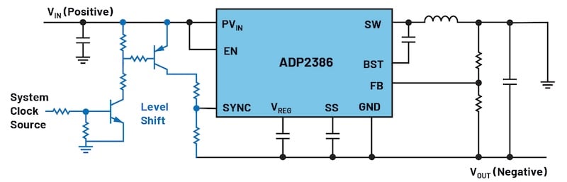
Figure 2. External level shifter for supplying the switching regulator IC with an external clock for synchronization. Image used courtesy of Bodo’s Power Systems [PDF]
The switching regulator IC ground becomes the generated negative voltage. All pins on the switching regulator IC are now referenced to the generated negative voltage rather than the system ground. As a result, the communication lines and connections from the system to the IC and vice versa need level shifting to guarantee safe communication and prevent damage. Typically, the relevant signals are SYNC, PGOOD, TRACKING, MODE, EN, UVLO, and RESET. Figure 2 shows a possible level shift circuit with two bipolar transistors and seven resistors (in blue) for one signal. This circuit requires a certain amount of space and adds complexity to the circuitry and costs. Such a level shifter would have to be implemented separately for all signals previously mentioned. It is especially complicated when a switching regulator IC uses a digital bus such as the Power Management Bus (PMBus). Then, the entire bus connection has to be operated with level shifting or galvanic isolation.
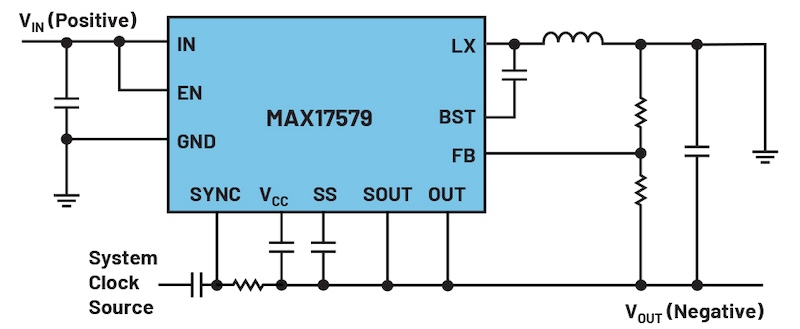
Figure 3. A MAX17579 is designed as an inverting buck-boost regulator with level shifting already integrated. Image used courtesy of Bodo’s Power Systems [PDF]
One way to avoid this external circuitry is to use a switching regulator IC that has been designed specifically for inverting voltages. Analog Devices offers a family of switching regulator ICs that are variations of buck regulator ICs. They are designed to facilitate communication between the system—the entire electronic circuitry and the inverting switching regulator IC. External level shifting, as shown in Figure 2, is not needed.
Figure 3 shows the MAX17579 switching regulator IC, which generates a negative voltage from a positive voltage. The circuit is much more compact than the one in Figure 2.
Simulation tools such as LTspice or the EE-SIM design and evaluation environment can provide a better understanding of the regulation behavior and potential differences in an inverting topology. These tools can also be used to design and optimize level shift circuits. The EE-SIM design tool also easily simulates ICs like the MAX17579.
This article originally appeared in Bodo’s Power Systems [PDF] magazine.