Facebook
 Google
 GitHub
 Linkedin
Integrated Capacitors Reduce Commutation Loop Inductance
This article highlights Vincotech MLCC SMD capacitors with X7R dielectric that significantly reduced switching devices voltage overshoot during turn-OFF.
Designers pursuing the right balance of price and performance to satisfy today’s demand for power-switching applications are cutting it close with inverters. And engineers are more likely to select parts with performance parameters in the neighborhood of the target specifications to gain a built-in design advantage. This is why margins between devices’ maximum electrical value and the application parameters are shrinking.
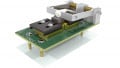
Power modules are a big step forward for engineers seeking to boost efficiency. They have several advantages over discrete components, one being superior parasitic performance. Nonetheless, there is still room for improvement, particularly if we take the electric components connected to the power module into consideration. These connections are still the source of parasitic inductances that adversely affect switching performance. They may even jeopardize the switching elements if the design lacks the necessary voltage buffer.
Parasitic inductance in an inverter power bridge leads to inefficiencies. The voltage spikes during the power device’s switch-OFF cycle (Figure 1) at a high rate of dI/dt:
$$V_{CD(peak)} = V_{CE} + L_x \times \frac{di}{dt} $$

Figure 1: Switch-OFF curves (Uce and Ic) of a power switch
Switching time may have to be increased to prevent voltage spikes from damaging power devices. Increasing power devices’ switching time would also increase turn-ON and turn-OFF losses in each power switch. This adds to the switching losses, generating even more heat to be dissipated in the switching devices.
DC link capacitors can mitigate the effects of inductance from the DC voltage source and reduce the switching component’s voltage overshoot. The key to good performance is a low-inductance design that connects these parts so as to minimize PCB and module pins’ stray inductance. Even so, the decrease in parasitic inductances is unremarkable no matter how carefully the designer configures this electric circuit. It certainly cannot compare installing a capacitor with a snubber function in the module (Figure 2). This integrated capacitor provides a low-inductive, high-frequency solution that closes the commutation loop.

Figure 2: Position of the snubber capacitor as it relates to the parasitic inductances of a module design
It is standard practice at Vincotech to integrate MLCC SMD capacitors. High voltage (650 -1000 V) parts in case size 1206 to 2220 can be applied as a snubber. Different types of capacitors may be used depending on the given specification. Devices with X7R (class2) dielectric materials have s higher capacitance in the same package as C0G/NP0 parts, but class 2 materials have a significant DC bias effect. This means that the part’s capacitance value is significantly decreased at the rated voltage (Figure 3).
_simulation_of_X7R_capacitor_showing_the_DC_bias_dependency_.jpg)
Figure 3: K-Sim (www.kemet.com) simulation of X7R capacitor showing the DC bias dependency
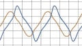
The comparative measurements of the SiC MOSFET booster configuration shown in figure 4 were taken to illustrate the behavior of the different setups, including one without a snubber capacitor. This test used a standard double-pulse measurement system and the MOSFETs’ nominal current. The switching devices were encapsulated in a standard Vincotech package with the additional snubbers placed on the layout by design.
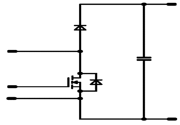
Figure 4: Booster configuration to test the integrated DC snubber effect
| option | value | overshoot (absolute value) |
| no capacitor | - | 205 (805 V) |
| X7R | 100 nF | 150 (750 V) |
| C0G | 22 nF | 121 (721 V) |
Table 1: SMD capacitor effect on overshoot voltage
The integrated capacitors significantly reduced the switching devices’ voltage overshoot during turn-off. This test also underscored the differences between capacitors’ dielectric materials. C0G/NP0 devices have significantly lower capacitances than their X7R counterpart and exhibited even better performance. This is attributable to the X7R class 2 material’s high DC bias effect.

Figure 5: Switch-OFF waveforms of the DC snubber effect test circuit. Yellow = gate voltage; green = collector-emitter voltage; pink = collector current
C0G/NP0 capacitors’ dissipation factor (DF) parameters are superior to those of the X7R, which results in less self-heating because of the dissipation factor’s lower ESR (equivalent series resistance) component.
Another advantage of the C0G/NP0 material is that it is immune to the aging phenomenon that causes the capacitance and dissipation factor of X7R devices to decrease over time.
About the Author
György Kovács received his Bachelor of Science (BSc) Electrical, Electronics and Communications Engineering, and Bachelor of Science (BSc)Business Administration and Management, General at Budapest Technical College, then College level postgraduate degreeEngineer specialized in Quality Management. He worked as a senior development engineer at Vincotech.
This article originally appeared in the Bodo’s Power Systems magazine.
Related Content