Facebook
 Google
 GitHub
 Linkedin
Serving 48V Power Systems With 100V GaN Discretes and Integrated Solutions
Learn how 100 V GaN devices are serving the needs of 48 V applications in data centers, renewable energy, and motor drives.
This article is published by EEPower as part of an exclusive digital content partnership with Bodo’s Power Systems.
If you search for ‘fast chargers’ on Amazon (other retailers are available!) almost all of the products that appear will be powered by a gallium nitride (GaN) switch. In this market, GaN has quickly become ubiquitous, and the term ‘GaN’ is even being used as a marketing shortcut for ‘efficient’, ‘high power density’ and ‘small size’. According to analyst company Frost & Sullivan, the GaN power market will grow at a CAGR of nearly 100% between 2024 and 2028, and will surpass $1B USD in 2026.
In addition to the mobile charger market, with the introduction of 100 V-rated products, GaN is also very suited to 48 V applications in data centers, renewable energy installations, and motor drives.

Image used courtesy of Adobe Stock
At a high level, the value proposition for GaN in these three markets is almost the same: high efficiency, high power density, and small size. GaN has two key characteristics that have led commentators to describe it as ‘the ideal switch’. It has a Figure of Merit (FoM – the multiple of the On-resistance, Ron, and the gate charge, Qg) which is 10 times smaller than best-in-class silicon, and it has no body diode, so reverse recovery current is zero.
Therefore, switching losses are minimal and efficiency is high. This means that power conversion systems can switch at higher frequencies, eliminating bulky passives and thermal management components, and simpler topologies can also be used. This reduces BOM count, leading to miniaturization or higher power from the same space.
With the introduction of GaN devices rated at 100 V from manufacturers such as Innoscience, the value proposition of GaN technology has been extended and devices are being implemented in fast growing 48 V markets. 100 V devices are needed for these applications, because ‘48 V’ is often a nominal description; the actual value may be 60 V or more. And a margin is always needed to cope with spikes.
Data Centers
Figure 1 shows the power management chain inside the data center, beginning with conversion from AC to DC, followed by 400 V DC to 48 V DC, and finally from 48 V DC to CPU/GPU supply voltages, which is the focus of this article.
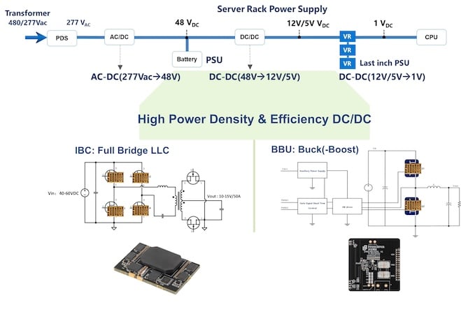
Figure 1. The 100 V GaN opportunity in data center power supplies. Image used courtesy of Bodo’s Power Systems [PDF]
To deliver power to the 48 V bus connection, there are two applications for 100 V GaN power ICs. One is a DC-DC converter (sometimes called an Interbus converter, IBC), which converts the 48 V distribution voltage to 12 V. The second is in the Battery-Backup Unit (BBU) for uninterrupted power supply. In both cases, the power levels range from a few hundred watts up to around one kilowatt. Because the GaN switch is so much faster than silicon with small losses, the frequency can be increased by a factor of five while maintaining elevated efficiency levels.
Higher switching frequencies reduce the size of passives, increasing power density. At the same time, power consumption can be reduced thanks to the improved system efficiency. The last step, from 12 V to 1 V, is also an application for GaN, which Innoscience addresses but is outside the scope of this article.
The power device innovation and demand is driven by Artificial intelligence (AI) market segment of High Performance Computing datacenters. GPUs of NVIDIA are the dominant technology used for AI computing, with continuously increasing power consumption within the same footprint (i.e. power density is going up) and strongly growing market size. We can illustrate the power consumption rapid growth on an example of NVIDIA GPU chips. These chips consumed around 300 W in 2018, increasing to 700 W now and the forecast is up to 1.6 kW power consumption by 2026. The power supply components dominate the overall footprint of a typical GPU module.
Renewable Energy
Traditionally solar panels are connected in a chain, and so if some devices are producing less power due, perhaps, to being in the shade, there can be a negative effect on the other panels. The optimizers track each solar module’s peak output and regulate voltage before the power passes to a central inverter. This increases efficiency, especially in partially shaded conditions and enables the performance of each individual panel to be monitored.
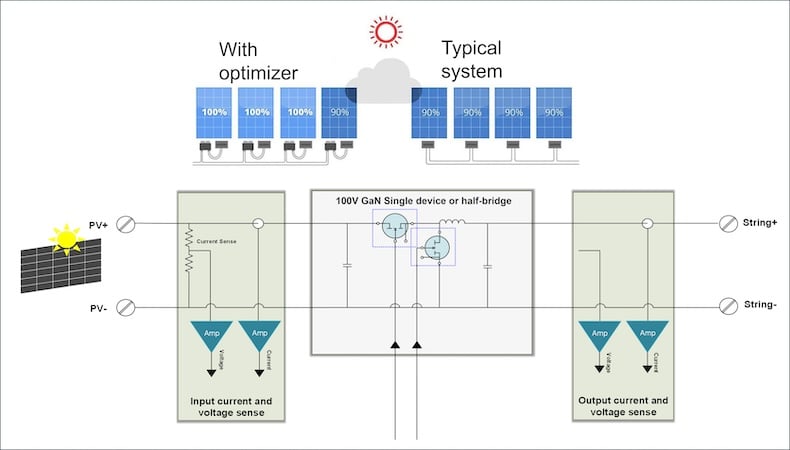
Figure 2. GaN power ICs help optimize solar optimizers. Image used courtesy of Bodo’s Power Systems [PDF]
Inside an optimizer, there is a hard-switching circuit that provides a power levels of up to about 1 kW. As with the data center PSUs, the key factor is to keep the size as small as possible. Robustness and reliability is critical since solar array installations may operate in the field for 25 years. Optimizers made using 100 V GaN ICs from Innoscience have been demonstrated to shrink the size of the unit by 70% when compared to silicon MOSFET solutions. Devices can operate at a peak efficiency of 99.2% and system cost is reduced by 30%.
Another renewable energy application for 100 V GaN power ICs is a bi-directional inverter for battery storage. In solar installations, any energy that is not directly consumed is stored in a battery for later use, which requires a bi-directional inverter.
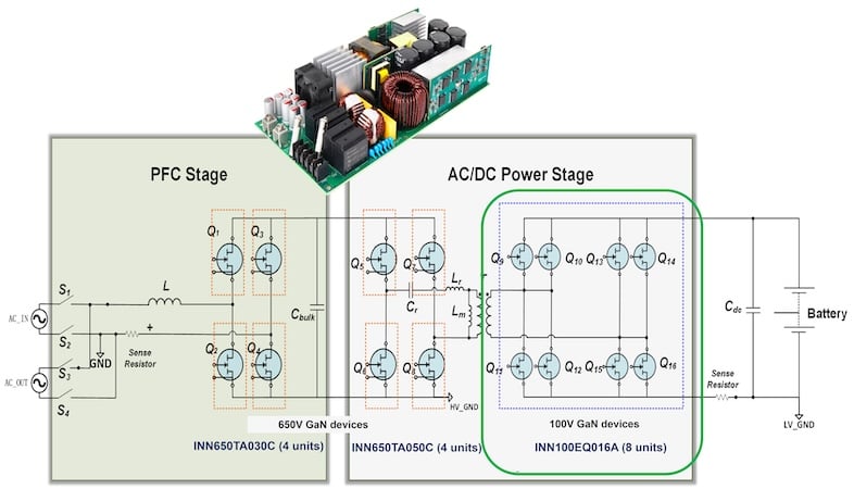
Figure 3. Example of best-in-class bi-directional inverter built using Innoscience 100 V GaN power transistors for solar / battery storage use case. Image used courtesy of Bodo’s Power Systems [PDF]
Our reference design for AC-DC power stage of a 2 kW bi-directional inverter built using Innoscience’s INN100EQ016A 100 V GaN power transistors (and other HV GaN devices) is as small as 248 x 120 x 45 mm3 and demonstrates peak efficiency of 96.1%.
Motor Drives
According to the IEA (International Energy Agency) “Electric motor-driven systems (are) the largest single-energy end use, (and) account for more than 40% of global electricity consumption.” (https://www.iea.org/reports/walking-the-torque) NETZERO policies create pressure to increase electrification leading to expectations of doubling the electric motor market size by 2033. However, electric motors can be shockingly inefficient, and noisy. We expect GaN devices to penetrate sub-1.5kW motor drives applications
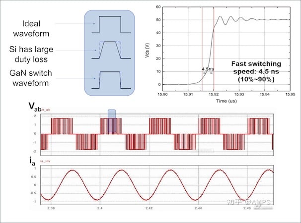
Figure 4. GaN’s near-perfect waveform reduces harmonic distortions and thus noise and also self-heating in electric motor drives. Image used courtesy of Bodo’s Power Systems [PDF]
The key differentiator of GaN in this application is its ultra-fast switching speed with near ideal square-like waveforms. This supports a short dead time and leads to a very low total harmonic distortion (Figure 4). These advantages are experienced by customers in low noise operation and low cost of BOM due to simpler filtering and smaller thermal management systems (e.g. heat sinks). The efficiency arguments for GaN, made elsewhere in this article, are equally applicable for motor drives. Overall GaN based motor drives are smaller, cooler, quieter and cheaper.
As an example, a 1000 W motor drive reference design has been produced replacing six MOSFETs and three controller ICs with just three SolidGaN ISG3201 half-bridge ICs from Innoscience. The unit operates at a high 98.2% peak efficiency (100 kHz), and the ripple current and total harmonic distortion have been reduced by 1.5x and 2.5x respectively when compared to the MOSFET-based implementation. Impressively, the PCB has also been footprint-reduced by 90%.
Innoscience Roadmap and Innovations
Innoscience is launching Gen3 100 V technology in early 2025. The Gen3 devices are leading figures-of-merits across the board (Ron*A, QG, QGD, QOSS, and gate and drain leakage currents), in particular QOSS and QGD will improve by 30% or more compared to Innoscience Gen2 production technology. The lead products are being released in LGA packages to support robustness and reliability, including on very thick PCB boards.
An example of application innovation is realization of 4 kW multiphase buck converter using discrete components on PCB board (as opposed to complex modules) using our lead 100 V Gen3 product INN100EA035A. This is RON max = 3.5 mΩ device in LGA 3.3 x 3.3 package. This buck converter is ideally suitable for 48 V to 12 V DC-DC conversion for power supplies in datacenter that has been discussed in the first part of this article. The design uses 64 GaN components, delivering 4 kW, multi-phase, 500 W per phase, and peak efficiency is above 98%.
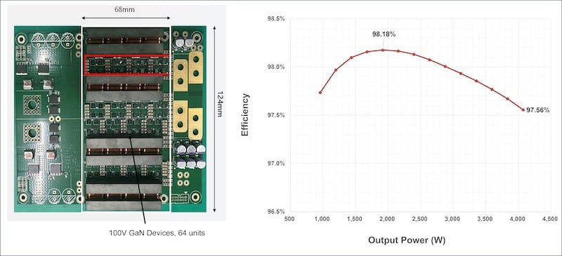
Figure 5. An example of 4 kW, multi-phase inverter (500 W per phase) using Innoscience’s latest 100V Gen3 technology INN100EA035A. The efficiency is measured with 54 V input, 12 V output at 250 kHz using heatsink and 400LFM airflow. Image used courtesy of Bodo’s Power Systems [PDF]
Conclusion
Innoscience offers a range of discrete GaN HEMTS and integrated half-bridge GaN ICs rated at 100 V which are well suited for the 48 V applications discussed. Our latest technology Generation 3 is in sampling stage and will be released for volume production in early 2025. The products using this technology will provide another leap forward in performance and system cost to all customers in the different market segments discussed in this article.
This article originally appeared in Bodo’s Power Systems [PDF] magazine.