Facebook
 Google
 GitHub
 Linkedin
Power Conversion with GaN-on-Si Integrated Circuits
This article details how the ascent of GaN is redefining power conversion.
Discrete power transistors, whether silicon-based or GaN-on-silicon, are entering their final chapter. GaN-on-Si integrated circuits offer higher performance in a smaller footprint with significantly reduced cost and less engineering required. This article details how the ascent of GaN is redefining power conversion.
Historical Perspective
In 1977, my colleague Tom Herman and I joined International Rectifier to start our professional careers in power conversion. Our initial project was to design a better power transistor compared with the power bipolar devices dominant in that era. After much evaluation and discussion, Tom and I settled on making a power transistor using a metal oxide (MOS) gate. Our first generation devices, with aluminum gate technology, launched in November 1978 and the second generation devices, based on silicon gate technology, launched in June 1979. Based upon their hexagonal structure, these second generation devices were dubbed the “HEXFET” and they started a massive redefinition of how power conversion was to be done.

IR's Eric and Alex Lidow: They believe they are two years ahead in technology
HEXFETs were faster, smaller, and eventually lower cost and more reliable than their bipolar ancestors. Designers needed to hone some of their engineering skills to take full advantage of the faster switching speed, which made power conversion systems, mostly AC/DC converters and motor drives at that time, smaller, more reliable and lower cost.
Tom and I recognized that designing with these new, higher-performing discrete devices would take precious time, and it was that design time that limited their rate of adoption. Our solution seemed simple: Develop integrated circuits that could be complete systems on a chip (SoC).
Our first attempt at creating a SoC was to build a monolithic triac using a recently invented device called TRIMOS [1]. Through this activity, we discovered some basic truths about integrating multiple power devices in silicon. By trying to put power devices that conduct vertically on the same chip, there was a significant increase in cost that prevented the SoC from being commercially viable. By making power devices lateral in design, the area consumed made the devices not commercially viable. Once this issue was known, Tom and a larger team, including Dan Kinzer and David Tam, pivoted and started developing driver ICs that could be used to switch power devices in half-bridge configurations. The first of these was the IR2110. To this day, discrete power MOSFETs (or their cousin, the IGBT) and driver ICs dominate the world of power conversion.
Gallium Nitride (GaN) Power Transistors
When I first heard about a team in Japan developing a method to grow device-grade gallium nitride (GaN) on a silicon wafer [2], I realized that the integration limitations of silicon in power conversion systems could be overcome with a new technology. GaN is naturally insulating, and the best way to make a GaN transistor is to have the three terminals, gate, drain, and source, on the top surface. There is no significant minority carrier conduction in GaN, so there would not be the problem of one power device polluting another with holes or electrons, as in lateral power MOSFET devices when they go into diode conduction.
![SEM micrograph of an eGaN FET circa 2009 [3.]](https://eepower.com/uploads/articles/Power_Conversion_With_Gan-On-Si_Integrated_Circuits_Figure_2.jpg)
Figure 1: SEM micrograph of an eGaN FET circa 2009 [3.]
Based on this understanding, my two colleagues Joe Cao and Bob Beach, and I founded Efficient Power Conversion (EPC) in the fall of 2007. From the beginning, the goal was to make power devices that are both higher performing and are lower cost than their silicon ancestors. Initially we set our sights on developing discrete devices, but we knew that integration would be a way to redefine power conversion in a meaningful way, much like integration redefined digital electronics, and the adoption of the HEXFET, decades earlier.
In 2009, we delivered our first prototypes of 100 V discrete GaN-on-Si power transistors. They were put into production in March of 2010, along with a family of 40 V and 200 V transistors. As enhancementmode devices, we named them eGaN® FETs. A scanning electron micrograph (SEM) image of these eGaN FETs is shown in figure 1.
These devices were fast – about five to ten times faster than silicon devices with the comparable voltage and on-resistance. This increased speed meant that circuit designers needed to be more careful with their layout, because added parasitic inductance would cause voltage and current overshoot. This overshoot increased power losses, increased EMI and EMC generation, and often led to designs that resulted in overvoltage of the gate or drain of the parts. The degree of difficulty designing with these parts seemed to be inversely proportional to the speed of adoption.
Within a year, we had established a second generation of products that were more stable with time and covered a wider range of applications including lidar, envelope tracking, vehicle headlamps, and DCDC converters. This experience taught us that we had a challenge – we needed to make it easier for designers to harvest the full capability of these leading-edge devices.
GaN Integrated Circuits
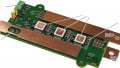
Our first step forward in the integration of functions on a single chip came in September 2014, when EPC launched a family of monolithic half-bridge devices. By integrating two FETs onto a single chip that could be configured as a half bridge, the customer could (a) save a lot of board space, (b) cut the power loop inductance in half, and (c) reduce overshoot that leads to EMI and EMC. Figure 2 shows an example of one of these early half-bridge ICs, which was designed for a DC-DC converter in a buck configuration. The high-side transistor was designed to be smaller than the low-side transistor, and it was designed such that the inductance between the two power devices was near zero. Figure 2: EPC first launched a monolithic half bridge in September 2014. (Shown is the EPC2100.)

Figure 2: EPC first launched a monolithic half bridge in September 2014. (Shown is the EPC2100.)
In parallel, work started on adding drivers to power FETs on the same chip. The monolithic devices with drivers would reduce the need for an external silicon-based IC driver and would eliminate gate loop inductance. The first commercial products were launched in 2018. An example is shown in figure 3.

Figure 3: Using GaN-on-Si technology, the EPC2112 (shown here) integrated a driver and a power FET for the first time.
The ultimate goal, however, was to integrate all necessary functions for a complete power conversion solution on a single chip. As there are many types of power conversion topologies, there are many types of possible solutions. However, there is one building block that stands out as the most common, the half bridge. Half bridges are used in buck converters, boost converters, LLC converters, bus converters, motor drives, and many more converter topologies. It is therefore a worthwhile endeavor to create integration around a half bridge. Figure 4 shows how all the pieces fit together.
Since GaN is naturally insulating, high-side and low-side FETs can be located next to each other. By reducing the distance between the gate and drain terminals, tiny low voltage FETs can be made next to high voltage FETs. These small-signal devices can be used to make analog as well as digital functions. The high side and the low side can be connected with a high voltage level-shifting device shown in figure 4 on the far left.

Figure 4: Illustration of how all the functions needed for a monolithic half bridge can be integrated on a single GaN-on-Si chip.
The first-generation EPC eGaN® ICs, such as shown in figure 3, were “handcrafted” based on trial-and-error and highly-educated guesses. To achieve the best and most reliable performance, technology platforms need to be translated into a rich set of models that scale, include parasitic interactions, are characterized over all temperature, voltage, and current conditions, and include realistic process variations. This is no small task, and it creates a natural tension with the simultaneous rapidly improving discrete FET performance. On one hand, it takes time and effort to fully characterize a technology platform; on the other hand, if the technology platform is changing faster than the characterization process, then the IC products lag their discrete counterparts in performance and cost effectiveness.
The initial output of this more formalized approach was first demonstrated in March 2020 with the introduction of a fully monolithic half bridge that integrated all the drive and level-shift functions, along with the bootstrap function. The simplified circuit diagram containing all the essential functions of a power stage is shown in figure 5, and the actual device photo is presented in figure 6.

Figure 5: All the basic functions of a power stage are shown in this simplified circuit diagram, including output FETs, drivers for these FETs, level shifting for the high-side circuitry, input logic and protection, and a synchronous bootstrap function to generate the voltage needed to drive the high-side circuitry.

Figure 6: The EPC2152 is a monolithic implementation of the circuitry in figure 5. It was designed for operation as either a buck converter up to 2 MHz with an input up to 80 V and an output of 10 A, or as a stage in a three-phase brushless DC (BLDC) motor drive operating at 100 kHz or more. The chip measures 10 mm2.
Although simple in comparison to modern digital processors, this single-chip power stage provides a first demonstration of the integration of many important fundamental functions. It includes comparators, a central building-block for decision making in an integrated circuit, feedback for control of output action, latching for isolation of input and output, ESD immunity for assembly robustness, and voltage isolation between high-side and low-side devices on a single substrate.
Nearly any IC can be made using just this set of building blocks. Although design refinement and improvement will continue at a rapid pace, this first demonstration shows the immense opportunity available for creating GaN ICs and the bright future gallium nitride has for redefining power conversion. This product from EPC (the EPC2152) was designed for use in buck converter or motor drive topologies.
Shown in figure 7 is the system efficiency of the monolithic power stage (green line) when operated as a buck converter at 1 MHz with 48 VIN and 12 VOUT at 10 A. The black “X” in figure 7 shows the comparative performance of a state-of-the-art silicon solution at 1 MHz. The GaN monolithic power stage achieves a 50% reduction in power loss versus the silicon solution.

Figure 7: The EPC2152 power stage operating at 1 MHz (green line) has an overall power loss (including inductor and control IC) at 10 A that is 50% lower than the best Si MOSFET solution (black X) when operated with 48 VIN and 12 VOUT. The blue line shows the comparative performance when the power stage is fabricated with discrete GaN FETs driven by a silicon IC
Also shown in figure 7, is the advantage gained by integrating the driver and the power FETs on the same chip. The blue line is the measured efficiency of the identical half bridge, but with discrete GaN FETs and the driver and level shift in a separate Si-based IC. The two main reasons for the significant improvement in efficiency are; (1) the reduced inductance in the gate loop when the driver and power devices are in intimate contact on the same chip, and (2) the monolithic integration of the two power FETs cuts in half the overall power loop inductance.
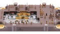
In addition to a buck converter application, the EPC2152 was designed to be used in the primary side of an isolated DC-DC converter or for BLDC motor drives, as shown in figure 8.

Figure 8: Three-phase BLDC motor drive using EPC2152 monolithic power stages.
The Future for GaN Integration
With a well-defined and rich set of scalable models based on the latest GaN technology platform, the challenge for further integration – the Ascent of GaN – shifts to adding even more functionality on a single chip [4]. The ultimate goal is to achieve a single component IC that merely requires a simple digital input from a microcontroller and produces a power output that drives a load efficiently, reliably under all conditions, in the smallest space possible, and economically.
To achieve this goal, sensors for current and temperature will need to be added to the chip. In addition, more digital control function will improve performance, lower cost, and reduce the overall engineering required of the power system designer. These added features and functions will become available over the next couple of years.
Discrete power transistors, whether silicon-based or GaN-on-Si, are entering their final chapter. Integrated GaN-on-Si can offer higher performance in a smaller footprint with significantly reduced, at lower cost with less engineering required. Figure 9 shows the projected journey toward a fully monolithic system on a chip (SoC) starting with the first monolithic half bridges in 2014 and continuing with multistage and multiphase ICs for all power conversion applications.

Figure 9: Efficient Power Conversion’s journey towards a fully monolithic system on a chip.
About the Author
Alex Lidow is CEO and co-founder of Efficient Power Conversion (EPC), former CEO of International Rectifier and is the co-inventor of the HEXFET power MOSFET, a power transistor. He has authored numerous peer-reviewed publications on related subjects, and received the 2015 SEMI Award for North America for the commercialization of more efficient power devices. Lidow was one of the lead representatives of the Semiconductor Industry Association (SIA) for the trade negotiations that resulted in the U.S. – Japan Trade Accord of 1986 and testified to Congress on multiple occasions on behalf of the industry.
References
- B. Scharff, James D. Plummer, “A MOS-controlled TRIAC Device”, IEEE International Solid State Circuits Conference Digest of Technical Papers 1978.
- Nakamura, S.,”GaN growth using GaN buffer layer,” Jpn. J. Appl. Phys, 30 (10A) L1705- L1707 (1991)
- A. Lidow, M. de Rooij, J. Strydom, D. Reusch, J. Glaser, GaN Transistors for Efficient Power Conversion, 3rd Edition, J. Wiley 2020. Available from https://epc-co.com/epc/Products/Publications/GaNTransistorsForEfficientPowerConversion.aspx
- A. Lidow, “Gallium Nitride Integration: Going Where Silicon Power Can’t Go [Expert View],” IEEE Power Electronics Magazine, Vol. 5, Issue: 3, Sept 2018. pp 70-72.
This article originally appeared in the Bodo’s Power Systems magazine.