Facebook
 Google
 GitHub
 Linkedin
Benefits of UL-certified Smart Gate Drivers in Advanced Power Converters
Through improvements in power switches and microcontrollers, the designers of power electronics can improve efficiency by up to another percentage point with each new generation of product they design. There is no limit to the number of applications benefitting from these advances, from electric vehicles with motor inverters and battery chargers to uninterruptable power supplies, servo drives, and solar inverters.
However, these improvements often require moving to higher switching speeds and changing from silicon IGBTs or MOSFETs to silicon carbide (SiC) devices. This introduces new challenges that must be resolved as engineers examine the impact of increased dv/dt and di/dt around the switches.
Various approaches for resolving such issues require the circuitry around the switches to be optimized. Challenges range from the effect of spurious turn-on caused by the non-linear Miller capacitance between the collector/drain and gate to responding to shortcircuits in or overloads of the switches. All resolutions to these issues take time to determine, resolve, and qualify. Instead, selecting an integrated smart gate driver with UL/cUL certification is often beneficial.
Dealing With Miller Capacitance
As switches are turned off, the Miller capacitance between the collector/drain injects current into the gate. Any series resistance between the gate and the driving circuit results in a voltage being developed that, worst case, can cause the switch to be turned on again. So, although IGBTs and Si/SiC MOSFETs are nominally off for a VGS or VGE of 0V, gate driver circuits often use a lower, negative voltage when applying the off state (Figure 1, left). This ranges from -5V for MOSFETs to -7V for IGBTs, thereby countering any gate-resistance-induced voltage rise.
Although this is a perfectly acceptable resolution to the issue, it does require an additional supply rail that may not be required in the remainder of the design. To avoid this, a Miller clamp circuit may be employed. By introducing an additional MOSFET between the gate and emitter/source, the gate voltage is clamped after the drive signal has transitioned below a pre-determined level (Figure 1, right). After the collector/drain has stabilized at its off-state voltage, this clamping switch can be disengaged. The timing of this step is not especially critical, but it must have been completed before the next on-state.

Image used courtesy of Bodo’s Power Systems [PDF]

Figure 1. To avoid the MOSFET being turned on again due to the Miller effect, the gate driver can pull the gate to a negative voltage (a) or clamp the gate to the emitter/source using an additional, in this case, external switch (b). Image used courtesy of Bodo’s Power Systems [PDF]
Protecting Against Overload Conditions
Power switches can fail when subjected to short circuits or when the applied gate drive voltage fails to push them fully into the saturation region. Monitoring the collector/drain voltage during the on-state allows the driver circuit to force the switch back into the off-state should a pre-defined threshold voltage be exceeded. This technique is known as de-saturation (DESAT). Because the shortcircuit withstand times are very short (a few milliseconds at best), this mechanism must respond very quickly. However, this is very challenging with devices switching at many kHz and in an electrically noisy environment.
Integrated gate drivers with a DESAT feature require a minimal number of additional components to implement such protection. In combination with a resistor-capacitor network, a diode is connected to the collector/drain on one side and the gate driver’s DESAT pin on the other (Figure 2). When the power device is saturated, the diode is forward-biased, pulling the DESAT pin low. By comparing this voltage with the gate driver’s VDESAT,max setting and drive state, the gate driver can determine if a fault condition has occurred.

Figure 2. Adding a diode together with an RC network, a smart gate driver can detect the saturation of a MOSFET via a DESAT monitoring pin. Image used courtesy of Bodo’s Power Systems [PDF]
The diode must be rated for the full DC bus plus some margin that can easily reach 1,000 V or more in some applications, although the forward-current rating can be low. The device should also be fast acting with very low capacitance and reverse recovery charge. Because these characteristics are difficult to find in a single diode, devices are often combined in series. This helps to increase the voltage rating while reducing the capacitance but increases the forward voltage drop and, in turn, the DESAT threshold detection. SiC diodes are also an option, but it should be remembered that they have a higher forward voltage than conventional silicon diodes.
To protect the DESAT pin, a Zener diode is the ideal choice for clamping the voltage to a level safe for the gate driver, while a Schottky diode can clamp the signal below ground.
Determining Components for DESAT Circuits
To start designing the DESAT circuit, the transfer characteristic of the MOSFET must be ascertained. From here, the resistor and capacitor for the DESAT circuit can be calculated. For example, examining the ID – VDS curve for a SiC MOSFET, the drain-source voltage for the normal and maximum operating point is determined for a fixed VGS, as shown in Figure 3, top.

Image used courtesy of Bodo’s Power Systems [PDF]

Figure 3. ID – VDS curve for a TW070J120B SiC MOSFET. Image used courtesy of Bodo’s Power Systems [PDF]
In the case of a TW070J120B, VDS is 1.1V at an ID of 20A, and VDS is 2.35V at a maximum ID of 40A.
The next step is to find the VF for the selected diodes. For two CRF03A fast recovery diodes, this is 2 × 1.4 V, as shown in Figure 3, bottom.
The final step is to determine VDESAT,max and ICHG from the chosen smart gate driver’s datasheet. For the Toshiba TLP5214A, this is 6.5V and 250µA, respectively. From here, the RDESAT can be calculated (Figure 4).
\[R_{DESAT}=\frac{V_{DESAT,max}-(n\cdot V_{F})-V_{DS,SAT}}{I_{CHG}}\]
\[R_{DESAT}=\frac{6.5V-(2\cdot 1.4V)-2.35V}{250\,\mu A}=5.4k\Omega\]
Figure 4. Equation to calculate the value of RDESAT.
All that remains is to calculate the capacitor for CBLANK. By using the short circuit withstand times for chosen SiC MOSFET, which are between 2 µs and 4 µs, this is determined in Figure 5.
\[R_{DESAT}=\frac{V_{DESAT,max}-(n\cdot V_{F})-V_{DS,SAT}}{I_{CHG}}\]
\[R_{DESAT}=\frac{6.5V-(2\cdot 1.4V)-2.35V}{250\,\mu A}=5.4k\Omega\]
Figure 5. Equation to calculate the value of CBLANK.
In operation, the short-circuit and over-current protection respond, as shown in Figure 6.

Figure 6. Waveforms showing the DESAT response to a short-circuit and/or an over-current condition. Image used courtesy of Bodo’s Power Systems [PDF]
Smart gate drivers such as the TLP5214A generate an isolated signal via a fault output pin, indicating the problem with the controller circuit as the soft shutdown is engaged (Figure 7). The controller can then determine the best course of action, such as attempting to turn on the power switch after a programmed delay to ensure that the average power dissipation is not excessive. Should the timings for DESAT blanking and soft shutdown be too long for the application, perhaps because peak load and noise are lower, designers can consider the TLP5214, which offers essentially the same characteristics but with shorter timing for these two parameters. Both devices provide a maximum ±4.0A peak output current and have a rail-to-rail output swing. For applications with lower peak gate drive current demands or should backward compatibility to previous gate drivers be needed, the TLP5212 is available, offering a maximum ±2.5A peak output current and non-rail-to-rail swing.

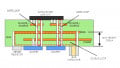
Figure 7. TLP5214(A) block diagram showing UVLO, Miller clamp, and DESAT features. Image used courtesy of Bodo’s Power Systems [PDF]
Available in an SO-16L package, creepage, and clearance of 8 mm are provided. With an isolation voltage of 5,000 Vrms(min), this family of smart gate drivers is suited to 600 VAC system voltages and meets the UL 1577 and EN 60747 safety standards. For IGBTs, switching frequencies of up to 50 kHz are supported, while SiC MOSFETs can be driven at up to 650 kHz. Delay propagation sits at ±150ns for the TLP5212 or ±80ns for the TPL5214 and TLP5214A. To support higher gate currents, the TLP5231 is a smart gate pre-driver, allowing design teams to specify their gate drive MOSFETs to scale to the application’s requirements.
Smart Gate Drivers Simplify Power Designs
Using discrete components, handling fault detection, and the impact of Miller capacitance in power designs is possible. However, such an approach requires board space and many parts, together with time to test and optimize the design. The design will also require safety certification. Smart gate drivers integrate all the necessary circuitry needed for DESAT fault handling and detection while avoiding the need for a negative supply, thanks to the Miller clamping capability. With the range of safety-certified gate drivers discussed here, scalable support is provided for a wide range of power demands both for traditional IGBT and silicon MOSFET designs and for those moving to high-speed switching using SiC MOSFETs.
This article originally appeared in Bodo’s Power Systems [PDF] magazine.
Featured image used courtesy of Adobe Stock.