Facebook
 Google
 GitHub
 Linkedin
From IGBT to SiC MOSFET A stone step for smooth replacement in Industrial Applications
This article highlights the advantages of transitioning to SiC MOSFETs from IGBT counterparts in terms of technical and economic aspects.
Features and benefits of silicon carbide (SiC) have been extensively demonstrated. It has been proven to be the suitable material for high voltage, high-frequency power switches. Several SiC-based devices have been launched in recent years.
Introduction
In an initial phase, in the early 2000s, Schottky barrier diodes (SBD) out of SiC have been implemented. SiC SBDs have been widely used in power factor correction (PFC) stage of single-phase switched mode power supplies (SMPS). They provided very low reverse recovery charge, saving a significant amount of dynamic losses in the diode itself and in the counterpart switch. Lately, further applications, like photovoltaic inverters and uninterruptable power supplies (UPS) also adopted SiC SBDs.

Figure 1: Timeline with main market events in the area of SiC devices
With respect to active switches, in 2010 the first normally-off silicon carbide switches were launched based on MOSFET structure. These devices simplified the gate driver circuitry, and enabled a smoother transition from standard silicon IGBTs and super junction MOSFETs. As consequence, many electronic companies from different application fields started to see SiC switches in their short term horizon and began development projects which include SiC MOSFETs. More recently, after extensive qualification procedure in system level, part of these projects turned out into products that were then introduced into the field.
There are however some particularities in the adoption of SiC MOSFETs. In order to get the maximum of their benefits, some changes in system design may be required. This article will describe some of the issues faced before and during the development phase. For each of these issues, some technical hints and, in some cases, practical examples will be shown in order to overcome these issues.
Quality and Reliability
One of the main concerns from development engineers is the reliability of SiC devices. This is understandable, since SiC does not have yet same time on the field than equivalent IGBTs and MOSFETs made out of silicon.
As it can be shown in Table 1, qualification processes of both silicon and SiC devices are following the same standards and test conditions.
ROHM also does innumerous further tests to verify the quality and lifetime of its products. Results of these tests can be directly shared with customers. In addition, when customer requires special tests outside standard conditions, they can be performed by ROHM after agreement.
Gate oxide lifetime
As shown in Figure 1, ROHM recently launched the 3rd Gen of SiC MOSFETs, first devices with trench gate, different from planar gate from former generations. This new structure practically eliminates the resistance from the parasitic JFET inside the structure. As a consequence, the amount of on-resistance per area unity has been reduced by half [2].
The trench structure adopted by ROHM, also known as U-structure, is shown in Figure 2 (a). As it can be seen, the electrical field around the interface SiC- SiO2 during blocking time is much lower than in the conventional trench structure. This guarantees a long lifetime of gate oxide, also for operation voltage levels close to nominal.

Table 1: Qualification tests of switches based on silicon and SiC materials.
1 Based on industrial standard tests for product qualification, as in „Semikron Application Manual“ [1]
2 From ROHM qualification of discrete parts, following JEITA ED-4701.
In order to turn the MOSFET on, voltage is applied between gate and source. As consequence, the electrical field occurs inside the gate oxide. In order to predict the lifetime of gate oxide, an accelerated test is performed, where higher voltage is applied to the gate. By collecting a certain amount of points with different gate voltages, it is possible to extrapolate the gate oxide lifetime when typical gate voltage is used. Figure 3 depicts results from an accelerated test of 3rd Gen SiC MOSFET from ROHM. It is possible to see that, for recommended gate values, lifetime of gate oxide is expected to be much longer than typical requirements industrial applications.

Figure 2: Double trench structure and simulated electrical field, compared to conventional trench
Considering further events, like short-circuit and avalanche, they have been proved through laboratory tests of SiC MOSFETs at ROHM. Definition of parameters like short-circuit withstand time (SCWT) and avalanche energy is now under preparation.

Figure 3 – Accelerated gate oxide lifetime test of 3rd Gen SiC MOSFET from ROHM, at Tj=175 °C.
In the meantime, short-circuit and avalanche shall be avoided, or solved in system level. This is already done for instance with silicon IGBTs, that inherently do not have avalanche robustness. Moreover, some ultrafast IGBT devices have also none or very reduced SCWT. Nonetheless, they have been widely used in industrial applications.
Robustness against Cosmic radiation
The phenomenon of cosmic radiation has been well described in the literature [3]. It can represent a critical issue, especially for applications which operate at voltage levels very close to the nominal voltage of the switch. This is the case for instance of photovoltaic inverters and UPS systems.
Failures due to cosmic radiation occur randomly during the lifetime of a semiconductor device. In accelerated tests, it is possible to predict the failure in time (FIT) rate of a device. This value is normally increasing exponentially with the blocking voltage, as shown in the test results in Figure 4. It shows the comparison between devices from silicon, namely IGBTs and MOSFETs, and SiC MOSFETs from ROHM semiconductor, all rated for same current and voltage. It is possible to observe that SiC MOSFETs have a FIT rate up to 3 orders of magnitude lower than silicon counterparts.
![FIT rate due to cosmic radiation for same current, same voltage rated devices from silicon (IGBTs and MOSFETs) and SiC MOSFETs. [3]](https://eepower.com/uploads/thumbnails/ROHM_Fig5_0.jpg)
Figure 4 - FIT rate due to cosmic radiation for the same current, same voltage rated devices from silicon (IGBTs and MOSFETs) and SiC MOSFETs. [3]
The reason of this huge improvement is due to some characteristics of SiC MOSFETs, which guarantee their robustness against cosmic radiation. Among them there is the smaller chip area of the device for the same current rate and the higher margin of electrical field during blocking state, with respect to breakdown field of the material.
Price-performance ratio
It is well known that the production cost of silicon carbide wafers is comparatively higher than those out of silicon. This is related, among other factors, to the energy involved in the growing process. This cost difference is expected to reduce sensitively in next years, driven by factors like:
- Increase of wafer size;
- Reduction of defect density on wafer level and those caused by processes;
- Economy of scale, following the increasing adoption of SiC devices.
Even facing higher price per device, it is already possible to build up systems based on SiC which offer economic advantages. Next section will discuss two examples of systems whose cost can be reduced by introducing SiC switches.
Auxiliary power supply
Industrial systems need an auxiliary power supply, which provides energy required to feed peripheral components, like micro-controller, gate drivers, fans, LCD displays, etc. For this application, Flyback converter is typically used. In 3-phase systems, where the input voltage can reach 480 Vac phase-to-phase, devices with blocking voltages above 1000 V are normally required.
Before availability of SiC switches, auxiliary systems were implemented with silicon MOSFETs and BJTs of up to 1500 V blocking capability. These devices present big chip area and still high on resistance. This results in high static and high dynamic losses, making the use of heat-sinks almost mandatory and increasing system cost.
With the use SiC, 1700 V rated MOSFETs offer on-resistance as low as 1 Ω. In addition, due to the small chip size, dynamic losses are sensitively reduced. As a consequence, it is possible to operate at switching frequencies up to 120 kHz ‑ thus reducing transformer size, - and still avoid the use of any heat-sink. This is demonstrated in [4], which also introduces the quasi-resonant controller for Flyback converters from ROHM.
Industrial power supply
Switched mode power supplies (SMPS) are widely used in industry to feed DC loads, like low voltage batteries. These systems are typically composed of two stages: an AC-DC rectifier followed by an isolated DC-DC converter.
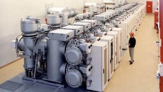
Figure 5 shows two industrial power supplies, disposed side by side. The system on the left is based on silicon IGBTs. It operates with switching frequencies of 20 kHz (AC-DC) and 40 kHz (DC-DC). Its achieved efficiency is 83% at the nominal power of 20 kW.
On the right side there is the new system, based on SiC MOSFETs. The much lower dynamic losses of these devices allowed switched frequency increase. The AC-DC stage operates at 40 kHz, and the DC-DC at 150 kHz. Considering all the consequent reduction in magnetic components, total system volume is 40 % smaller than reference system. Furthermore, there was no system cost increase, while the nominal power could be increased 30%, up to 26 kW.

Figure 5 – comparison between SMPSs made out of silicon IGBT (left) and SiC MOSFETS (right). Table aside shows circuit parameters and most important achievements with SiC-based system.
Electromagnetic Compatibility
SiC switches is to allow high frequency, high-speed switching. This kind of operation results in very low dynamic losses, but can also bring some challenges in accomplishing electromagnetic compatibility (EMC) requirements.
The standard CISPR11, - and especially its “B” version, dedicated to grid-connected systems – establishes limits for the electromagnetic interference (EMI) in the frequency range starting from 150 kHz. Frequency range and emission limits in dBµV are depicted in Figure 5.
Let a photovoltaic inverter be considered, operating under 20 kHz, typical frequency for silicon IGBTs above 600 V blocking capability. The squared waveform voltage coming from the inverter needs to be filtered before reaching the grid. This waveform can be described according to Fourier transformation as a series of sinusoidal waves, whose frequencies are the fundamental i.e. 20 kHz, and the odd harmonics, i.e. 60 kHz, 100 kHz, and so on. It is possible to demonstrate then, that the first frequency to fall into the regulated range is the 9th harmonic, which is naturally damped by almost 20 dBµV. This has been well depicted in [5], and is reproduced in Figure 6.
![Filtering effort for a grid-connected photovoltaic inverter, for different switching frequencies. As reference, the standard CISPR11 “B“ [5] modified.](https://eepower.com/uploads/thumbnails/ROHM_Fig7_0.jpg)
Figure 6 – Filtering effort for a grid-connected photovoltaic inverter, for different switching frequencies. As reference, the standard CISPR11 “B“ [5] modified.
If frequency is now increased to f.i. 100 kHz, the 3rd harmonic will already fall into the regulated area. As a result, there will be around 18 dBµV less natural damping, which must be compensated by a passive filter. In order to avoid system cost increase due to extra filtering effort, it is recommended to operate at switching frequency just below 50 kHz (3rd harmonic out of regulated range) or still slightly below 150 kHz (1st harmonic out of regulated range).
If higher switching frequency is desired, according to [5] the next sweet spot will fall above 400 kHz. Above this value, the size of the passive filter will be again smaller.
Parasitic elements as stray inductances, capacitances and resistances from the surrounding may block operation at such high frequencies. They may come, for instance, from packaging, isolation foils, capacitor series resistance, PCB design, among others. In order to overcome this issue, resonant topologies may be an interesting option. Circuits like series resonant LLC [6] avoid hard switching operation, reducing thus the emitted electromagnetic radiation. In addition, switching speed can also be controlled. This makes the voltage waveform more trapezoidal-like, and increases the natural dumping of the high-frequency harmonic content.
Conclusion
SiC MOSFETs brings significant technical improvement with respect to equivalent silicon devices. In addition, SiC MOSFET devices have already achieved the required quality level for most common industrial applications. This is proven by results of the standard qualification process and accelerated tests of gate oxide lifetime. In addition, SiC MOSFETs have improved robustness against some events, like cosmic radiation.
Economic advantages brought by SiC MOSFETs have also been demonstrated in some applications, even with the price difference as it is today. In the near future, factors like wafer increase and economy of scale will decrease the price of SiC devices and make it more and more competitive and practically all applications inside the electronic industry.
About the Author
Vladimir Scarpa is working as a Field Application Engineer at ROHM Semiconductor, an electronic parts manufacturer company with its main branch based in Kyoto, Japan. He was born in Uberlândia, Brazil, in 1980. He received the B.Sc. and M.Sc. degrees in electrical engineering from the Federal University of Uberlândia, Uberlândia, in 2003 and 2005, respectively. His research interests include power electronics applied to renewable energy sources and digital control of switching power supplies.
References
- "Semikron Application Manual", 2nd edition, page 117. Available online https://www.semikron.com/dl/service-support/downloads/ download/semikron-application-manual-power-semiconductorsenglish-en-2015
- “ROHM Semiconductor shows 3rd Generation SiC MOSFETs with Trench Gate Structure”. Available online http://www.powerguru. org/rohm-semiconductor-shows-3rd-generation-sic-mosfets-withtrench-gate-structure/
- Source : H. Asai, I Nashiyama, K Sugimoto, K Shiba, Y Sakaide, Y Ishimaru, Y Okazaki , K Noguchi, T Morimura “Tolerance Against Terrestrial Neutron-Induced Single-Event Burnout in SiC MOSFETs” IEEE Trans. Nucl. Sci., vol.61, 2014.
- Application Note “BD768xFJ-LB series Quasi-Resonant converter Technical Design”. Available online.
- A. C. Schittler, D. Pappis, P. Zacharias: “EMI filter design for high switching speed and frequency grid-connected inverters”, EPE 2016.
- Y. Nakakohara, et al “Three Phase LLC Series Resonant DC/DC Converter Using SiC MOSFETs to Realize High Voltage and High Frequency Operation”, IEEE Transactions On Industrial Electronics.
This article originally appeared in the Bodo’s Power Systems magazine.