Facebook
 Google
 GitHub
 Linkedin
Design and Optimization of Silicon Carbide Schottky Diode
This article highlights WeEn Semiconductors WeEn NXPSC0465 device for design and optimization of Silicon Carbide (SiC) Schottky Diode.
Silicon Carbide (SiC) is widely used in the medium/high voltage power semiconductor device manufacturing due to its inherent material properties of the wide bandgap and high thermal conductivity.
Nowadays, Schottky Diode, MOSFET and JFET are the most popular SiC power devices in the market, especially the SiC Schottky Diode, which already has almost 20 years of mature application experience when it was commercialized since the beginning of this century. The earliest SiC Schottky diodes employed a pure Schottky Barrier Diode (SBD) structure, then it evolved into the structure called Junction Barrier Schottky (JBS) with low reverse leakage current, and the newest structure is called Merged PN Schottky (MPS) exhibiting massively increased surge current handling capability.
WeEn Semiconductors released 650V SiC MPS Diode based on 100mm SiC wafer in 2014, and 650V SiC MPS Diode based on 150mm High-Quality SiC wafer in 2017. Earlier this year, based on the mature 150mm wafer technology, WeEn launched 1200V SiC MPS Diode and AEC-Q101 qualified 650V automotive SiC MPS Diode.
In this article, we will firstly discuss the reason why SiC power devices possess superior performance, then share the design process of SiC products. At last, WeEn SiC MPS diode featured ultra-low reverse recovery charge (Qrr) will be introduced.
Why are SiC Power Chips Smaller?
The size of the power chip is directly determined by the on-resistance per unit area, and the on-resistance is mainly dominated by the resistance of the epitaxial layer which acts as the functional layer. To minimize the device on-resistance, it is necessary to either increase the dopant concentration (i.e. lower the resistivity) in the epitaxial layer or reduce the layer thickness, but these will also result in the degradation of breakdown voltage. That means the chip designer must trade off the on-resistance and the breakdown voltage well.

Figure 1: Electric field profiles comparison of SiC and Si devices at the same blocking
According to Poisson’s equation, the device breakdown voltage is proportional to the square of the breakdown electric field (VB∝B 2). Due to having nearly 10 times higher breakdown electric field than silicon, SiC devices exhibit dramatically “friendlier” (i.e. lower resistance) epitaxial layer specifications range than silicon devices to achieve the same breakdown voltage rating. Taking 600V Schottky diode, for example, the epitaxial layer with 5um thickness and 1016cm-3 doping concentration is quite enough for SiC diode. But for silicon diode, the requirements for epitaxial layer specifications are much “more strictly” (i.e. higher resistance), at least 50µm thickness and 1015cm-3 doping concentration are needed. Undoubtedly, to avoid the further increase of epitaxial layer resistance, the only way is to expand the chip size. Therefore, thanks to the strong forward current conduct capability, the SiC power device can be designed to smaller chip sizes.
Why do SiC Power Chips Perform Better Under High Temperatures?
The intrinsic carrier concentration of Si is approx. 1010cm-3, while SiC only features 10-9cm-3, and both values are attained at room temperature. The most significant characteristic of intrinsic carrier concentration is that it will increase exponentially when the temperature linearly increases though. It can be seen, when the junction temperature reaches 200°C the intrinsic carrier concentration of silicon will exceed 1014cm-3 which the value is comparable with normal PN junction concentration, and this often induce the failure of the working silicon device irreversibly. Thanks to the ultra-low intrinsic carrier concentration, the SiC power device will undergo much higher temperature safely which even exceeds 600°C.
This is the main reason why SiC devices can withstand high temperatures. However, due to the limitations of packaging technology and application, the most common commercial silicon carbide products only show the highest junction temperature of 175°C in the product manual. Nevertheless, owing to three times higher thermal conductivity than silicon still makes SiC power devices exhibit much better thermal performance.
Why do SiC Diodes Have Better Switching Performances?
Most of the SiC diodes we talked about in the market are Schottky diode. As a unipolar device, Schottky diodes behave near-zero reverse recovery time, which means Si Schottky diode is also able to perform similar performance. But as we mentioned previously, high voltage Si Schottky diode will also exhibit huge on-resistance, which restricts the voltage rating of commercial Si Schottky diode to below 200V. For SiC, in contrast, the 650V/1200V/1700V SiC Schottky diode has been released to the market for a long time.
The conventional high voltage Si diode is a PiN diode in which high resistivity and thick epitaxial layer are used to withstand the high reverse voltage. The ON-resistance can be reduced by the injection of minority carriers from the P area (i.e. conductivity modulation), which is a common design to get high voltage Si diode. But this PiN type diode needs to spend extra time to remove the minority carriers and resulting in reverse recovery current when the device turns OFF. To make matters worse, the reverse current will be larger when the temperature increased due to the feature of minority carriers.
Owning to the nature of the Schottky structure, the reverse recovery behavior of the SiC diode will be independent of the temperature. In a word, due to the superior physical properties, the Schottky structure is available in high voltage SiC diode design, and thereby the SiC diode has much better switching performance.

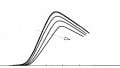
Figure 2: Reverse recovery behaviors of the Si PiN diode and SiC Diode at 125°C
In the last decades, SiC device manufacturers have been working hard to compare its performance with silicon devices, and the result is well known. However, SiC device designers cannot just satisfy with SiC devices ahead of Si counterparts, which in fact are mainly contributed by the material advantage. Even if equipped with the same SiC material, different manufacturers may exhibit different performances due to varied process capability and chip design involvement. Designers should make the most effort to achieve SiC devices which not only perform better than silicon devices but also the best in all SiC players’ devices.
Design
With a heritage of over 50 years, WeEn has abundant experience in power semiconductor devices design. The design process including: set the design goals based on customer need, device and process simulation using EDA tools but based on the foundry capacity, mask and process design, fabrication in the foundry, assembly, reliability testing. After several rounds of trial, optimization, life testing, and application testing, the qualified products with the optimal design are finally achieved.
Process Simulation
Due to the robust Si-C bond strength, high implant energy is employed to form PN junction in SiC. And since most implanted impurities (e.g. Al+) exhibit little diffusion in SiC even during post-implantation annealing, the implant energy, and dose must be designed precisely to achieve targeted doping profile, which is usually implemented by several steps, thereby simulation is needed in the implant process design. Designers can use Monte Carlo models in simulation to design the optimal implantation recipe to reach their target. It is also necessary to use the Secondary Ion Mass Spectroscopy (SIMS) method to measure the actual impurities profile after post-implantation annealing. The correction between simulation result and measurement value is an important step in chip design and manufacturing, especially when the recipe changes or new process equipment introduced.
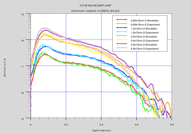
Figure 3: Simulated impurities profile and SIMS impurities profile of different implant energy (Figure captured from Silvaco)
Chip Architecture Design
To pursue the best device performance, a merged PN Schottky (MPS) structure is designed in all WeEn SiC Schottky diodes, in which the built-in voltage of the PN junction will be overcome earlier at high forward currents than the conventional JBS structure. Then the minority charge carriers injected into the drift region which the resulting in ON-resistance will decrease significantly, thereby the device is able to withstand higher surge current. But increasing the PN area will lead to less Schottky area, the on-resistance will increase at nominal forward current when the bipolar mode has not turn-ON.
Thereby there is a tradeoff between the normal forward conduct capability and the surge current handling. With the special P+ islands layout design and exclusive ohmic contact process, special surge current conduct paths are designed in WeEn SiC MPS diodes, which exhibiting superior surge current handling without any loss of nominal current conduction capability.

Figure 4: Schematic cross-section of WeEn SiC MPS diode and the current distribution

Figure 5: Comparison between forwarding I-V characteristic of WeEn NXPSC04650 4A, 650V MPS diode, and other company’s JBS diode at 25°C
Wafer Thickness Design
The power device suitable SiC wafer consists of two layers: the thick substrate layer and the thin epitaxial layer which grow on it. Owing to the thick substrate layer, SiC wafer, especially with large dimensions, exhibits better mechanical stability which is very important in the semiconductor process or shipping. But as we talked before, since the whole blocking voltage is suffered by the epitaxial layer, the substrate layer has no electrical function except as a current path which more like a series resistance.
Due to the commercially available SiC substrate cannot have high doping concentration, the substrate resistance is noticeable especially for 650V SiC device which features lower epitaxial layer resistance than higher voltage devices. The resulting power dissipation is undesired, to address this problem, grinding the substrate layer is considered.
But concerning the hardness of SiC material, there are several challenges to the manufactures including the possible cracks, surface roughness, and the thickness uniformity after grinding. Due to the leading manufacturing process and excellent quality control, WeEn SiC products all feature thin wafer design which performs only 1/3 substrate thickness of the standard products in the market. With the benefit of thin wafer design, WeEn SiC diodes have much better forward current conduction capability and lower thermal resistance.

Figure 6: Comparison between WeEn thin SiC product and the standard product from other company
Manufacturing Management
Rigorous production management and quality control are essential steps to guarantee the stability of product performance. To provide customer highest reliable SiC diode products, WeEn has built comprehensive quality and reliability control systems and programs. All SiC products have to go through 100% static parameters testing, 100% surge current handling testing (IFSM) and 100% avalanche capability testing (UIS), also needs to follow the JEDEC standards or even more strict reliability testing items, like extending the HTRB testing period from 1000 hours to 3000 hours.
Optimization
Compare to the bipolar silicon fast recovery diode (FRD), SiC Schottky diode belongs unipolar device with majority carriers only. Due to no minority carriers exist in normal operation, there is not any recombination or removal of minority carriers and resulting reverse recovery current. In high-frequency application, SiC Schottky diode can switch very fast with much lower switching losses than Si FRD.
Product Introduction
Near-zero reverse recovery current, this is the most frequent description we can find in the datasheet of SiC Schottky diode. However, “near” means there is still some recovery current of SiC Schottky diode which also observed in actual testing. This is caused by the charge and discharge procedure of junction capacitance though there are not any minority carriers.
The reverse recovery charge quantity of SiC Schottky diode has a relationship with the active cell quantity and concentration of the epitaxy layer, which these parameters also determine the forward voltage drop, blocking voltage and leakage current, tradeoff is needed in design. We can find the different reverse recovery performance of SiC Schottky diode from different suppliers because they use different chip designs.
| Product | Qrr (nC) |
| If = 10A, di/dt = 500A/μs, VR = 400V, T = 25 °C | |
| WeEn NXPSC10650 |
14.3 |
| Company A 650V 10A SiC Schottky Diode |
15.2 |
| Company B 650V 10A SiC Schottky Diode |
23.9 |
| Company C 650V 10A SiC Schottky Diode |
24.2 |
| Company D 650V 10A SiC Schottky Diode |
28.5 |
| Company E 650V 10A SiC Schottky Diode |
33.8 |
Table 1: Qrr Comparison of WeEn MPS diodes and commercially available SiC Schottky diodes
Due to the optimal active area design and leading manufacturing process, WeEn SiC Schottky diodes not only have standard level static parameters but also feature leading industry reverse recovery performance in the field, exhibit excellent high operation frequency performance.
Experiment
The typical application of SiC Schottky diode is acting as a boost diode in the PFC (Power Factor Correction) circuit. Especially under CCM (Continuous Current Mode) operation, when the PFC switching transistor turn ON, the boost diode will switch OFF, and the reverse recovery current which formed by the recovery charge will inject into the switching transistor. Due to the voltage drop of the transistor is still high when it is switching ON, the injected reverse recovery current will cause high power losses. The more the reverse recovery charge, the higher the resulting energy dissipation. Thanks to having only a 60% reverse recovery charge than most products in the market, WeEn SiC Schottky diodes dramatically reduce the generated energy dissipation.

Figure 7: CCM PFC circuit and the energy losses at turn-ON
To show the superiority of WeEn products, using NXPSC08650 8A, 650V SiC MPS diode to replace the original 10A SiC Schottky diode of Company X which is used in the PFC circuit of an 800W server power. Under 70kHz work frequency, the server exhibits higher energy efficiency than its original design using a more expensive 10A SiC Schottky diode. Benefit by the ultra-low Qrr performance, the power server using WeEn SiC Schottky diode will have more excellent efficiency performance at a higher operating frequency.
Conclusions
Thanks to its excellent material property, SiC Schottky diodes perform much better than silicon diodes. Combined with advanced chip design capabilities and mature manufacturing processes, the best of the SiC Schottky diode will be achieved.
| Diode | NXPSC08650 | XXXX10650 |
| Efficiency | 98.90% | 98.79% |
Table 2: Efficiency results of power server using NXPSC08650 and other company’s 10A device
About the Author
Alex Cui received his Electrical Engineering degree at Hefei University of Technology and Masters in the field of Power Electronics at Zhejiang University. He worked as a Senior Development Engineer at WeEn Semiconductors company that is a key player in the semiconductor industry and has focused on developing a wide and deep portfolio of industry-leading bipolar power products including silicon carbide diodes, thyristors - consisting of silicon controlled rectifiers and triacs, high voltage transistors and so on.
References
This article originally appeared in the Bodo’s Power Systems magazine.
Related Content