Facebook
 Google
 GitHub
 Linkedin
Experimental Results of Isolated Flying Capacitor Multilevel Converter Frequencies and Loads
This article presents the experimental results of isolated flying capacitor multilevel converters, including tests at different frequencies and loads.
To catch up on this series on Isolated Flying Capacitor Multilevel Converters, follow these links:
- Isolated Flying Capacitor Multilevel Converter Basics
- Isolated Flying Capacitor Multilevel Converter Modes of Operation
- Hardware Design of Isolated Flying Capacitor Multilevel Converters
An isolated flying capacitor multilevel converter (FCMFC) is a power converter that uses flying capacitors to achieve high voltage conversion ratios. The FCMFC operates by charging and discharging the flying capacitors in a sequence to generate multiple voltage levels, allowing for higher output voltage with fewer components than traditional converters.
Experimental Results
Each converter underwent tests at frequencies of 100 kHz, 250 kHz, 452 kHz, and 500 kHz with an increasing constant current load, a set duty cycle of 5 V, and a blanking time of 1 μs. Starting with a very low load (<10 mA) and gradually increasing by 50 mA until the maximum load. Together with the flying capacitor voltages, input, output voltage, and current were all measured at each location.
Operation and Voltage Balance
The 50 MHz Yokogawa DL850E oscilloscope used probes from Yokogawa 700929 and Rigol PVP2150. Figure 1 shows the 5 V to 40 V, 250 kHz case recorded for the N4 converter. The signal that drives the primary FET gate is shown in blue at the top, while the voltages of the two flying capacitors are shown in pink (C1) and green (C2), and the output voltage is shown in red. Note that these are not differential measurements. Instead, they are taken from the flying capacitor positive node to the isolated secondary side ground.
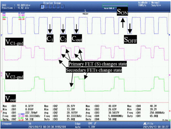
Figure 1. N4 flying capacitor charging action. Image used courtesy of IEEE Open Journal of Power Electronics
For the flying capacitors, the time scale is 5 μs/div, and the voltage scale is 10 V/div. When the blue gate signal drive goes low, the charging action of the secondary side flying capacitor will happen. The magnetizing inductor will first charge C1. A black arrow on the blue gate drive signal shows how this will happen. Because the voltage ripple ∼1 V, C1 charging is not visible, but it is being done as shown. In the next cycle, the inductor is connected to C1 in order to charge C2. This is clear on the C1(pink) voltage waveform because the measured voltage is pulled up to the C2 level.
Next comes the output stage, where the output capacitor is charged by the inductor with C2. With a 2.5% ripple, the green measurement now matches the output voltage of 40 V shown in red. Again, the actual ripple voltage of each capacitor is 1 V, and what is shown in the figure are measurements to ground. This means that the changes shown are changes in switching states. As shown in Figure 1, there is a change in voltage when the secondary switches change states and again when the primary FET switches ON or OFF.
At each stage, the flying capacitor voltage was measured to check the charging action and voltage balance. Figure 2 is a voltage plot for the N4 converter, which has two flying capacitors (C1 and C2) and an output capacitor (Cout). For a 14 W power output, the voltages were measured every 50 mA. The voltage between the flying capacitors stays between one-third and two-thirds of the output voltage at each point.
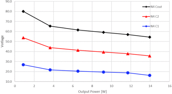
Figure 2. Experimental N4 flying capacitor charging action and natural voltage balance. Image used courtesy of IEEE Open Journal of Power Electronics
At the 9 W point, for example, the voltages for C1, C2, and Cout are, in order, 20 V, 40 V, and 60 V. When compared to the flyback converter, C1 is closest to the secondary coil and keeps the primary reflected voltage. This is cut to one-third of the output voltage. Load step-response is not shown because steady-state performance is being compared to dynamic performance. It is expected to be similar to other multilevel converters.
Voltage Gain
The predictions made in Equation 1 and Figure 3 are accurate. Figure 4 shows that a sweep of the duty cycle from 50% to 90% under no load with a 5 V input was done to see how much gain each converter could have. The N3 converter has about twice as much voltage gain as the flyback converter, while the N4 converter has about three times as much. For example, with a duty of 85%, the flyback has a gain of 10, the N2 is 20, and the N4 is 32.
Also, the flyback converter's switching limit is usually around 90%. After 85%, the flyback voltage gain starts to go down, going from 10 to 8 at 90%. The gain of both FCMFC (flying capacitor multilevel flyback converter) converters stays between 85% and 90%, but the N4 device is more important. The N2 goes up from 20 to 21, and the N4 goes up from 32 to 37. Note that even with a higher turns ratio, the FCMFCs would still double and triple the voltage gain that a flyback can achieve.
\[M(D)=\frac{V}{V_{in}}=\frac{n(N-1)D}{1-D}(1)\]
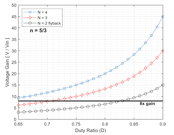
Figure 3. Ideal voltage gain vs. duty cycle for flyback converter and FCMFC. Image used courtesy of IEEE Open Journal of Power Electronics
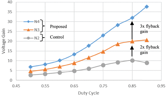
Figure 4. Experimental unloaded voltage gain to be compared to Figure 3. Image used courtesy of IEEE Open Journal of Power Electronics
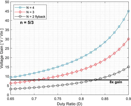
Figure 5. Non-deal voltage gain for the flyback converter and FCMFC for a 160 Ω load. Image used courtesy of IEEE Open Journal of Power Electronics
Figure 6 is a graph of output power versus voltage gain that shows how loading affects voltage gain. Each converter with a 5 V input has a fixed switching frequency of 250 kHz and an effective duty cycle of 72.5%. As expected, the flyback gain stays at 4, the N3 is doubled to 8, and the N4 is tripled to 12. The voltage gain of an FCMFC is always twice, three times, etc., that of a flyback converter.
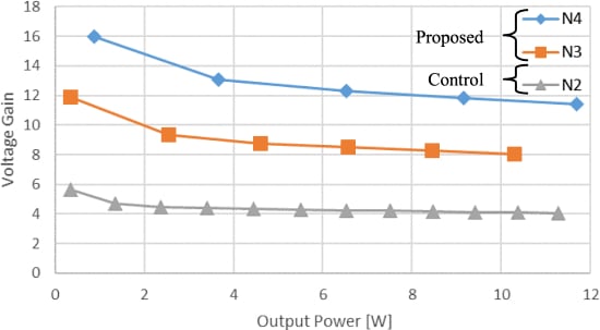
Figure 6. Experimental loaded voltage gain. Figure 5 is used to validate this plot, but with D fixed to 72.5%. Image used courtesy of IEEE Open Journal of Power Electronics
Zener Snubber Loss
The FCMFC converters will have about one-third of the zener snubber loss of the flyback converter. To show this, the N2 and N3 converters were run at a load of 8 W until they reached a stable temperature, shown in Figure 7. The zener diode is the white area that is the hottest in both pictures. The temperature goes up to 156 °F for the flyback converter, but it only goes up to 86 °F for the N3. The same thing happens when the N4 converter is used. The voltage across the output capacitor on the flyback converter is half of what it is across the flying capacitor that is directly connected to the secondary coil. This voltage is returned to the primary when the FET is turned OFF, making the zener lose more power.
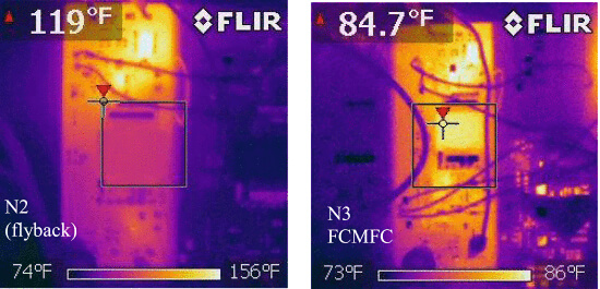
Figure 7. Thermal images of N2 and N3 at 8W load. Image used courtesy of IEEE Open Journal of Power Electronics
Efficiency
Figure 8 shows converter efficiency with 5 V to 40 V at 250 kHz. The calculation of efficiency considers all onboard circuitry, such as the auxiliary power, primary gate driver, isolated gate driver, etc.
Only the power the microcontroller uses, which is the same for all three converters, is considered. The FCFMC converter is more efficient than the flyback converter over the same range of loads. The best flyback efficiency is 75.6%, the best N3 efficiency is 85%, and the best N4 efficiency is 85.5%. The FCMFC converters are achieving higher efficiencies while having more switching devices and supporting circuitry. A plan was made to show that the circuit worked, relative efficiency increased, and to directly compare a flyback converter to the proposed FCMFCs. It was also made to show that relative efficiency went up.
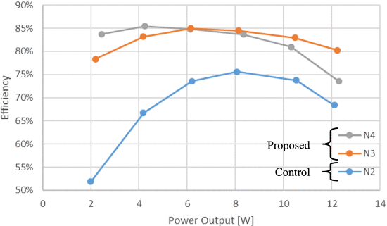
Figure 8. Efficiency vs. Output Power N2, N3, N4. Image used courtesy of IEEE Open Journal of Power Electronics
FCMFC converters (N3 and N4) can also work with a lower duty cycle and still have a higher gain range. For operations at 100 kHz, 452 kHz, and 500 kHz, the efficiency was the same. Switching losses increase when users operate at a higher frequency, so efficiency decreases slightly. Table 1 shows the results of tuning the duty cycles so that the converters could produce a 40 V, 10 W output at 250 kHz to compare their application capabilities.
Table 1. Efficiency At 5 V to 40 V, 10 W Load, 250 kHz
|
N |
Duty Cycle |
Efficiency |
|
2 |
82.5% |
77.72% |
|
3 |
72.5% |
84.74% |
|
4 |
66.0% |
81.57% |
The efficiency of the flyback converter is 77.72%, while the efficiency of the N3 converter is 84.74%. Because the flying capacitor lowers the secondary coil voltage, the zener snubber loss reduction shown thermally in Figure 7 makes the FCMFC more efficient. The N4 converter has the same benefit, but its efficiency is lower at 81.57% because the extra flying capacitor stage adds more conduction and switching losses. Future versions of this converter can use FETs with lower ratings and reduce conduction losses even more, making them much more efficient.
Isolated Flying Capacitor Multilevel Converter Summary
This work has demonstrated how the FCMFC works for two cases, N3 and N4, and an N2 or flyback converter design. The same transformer and semiconductor parts were used to remove bias in comparison. Since experiments have shown that the FCMFCs work better than the flyback converter, it is clear that any optimization would lead to FCMFCs that are more efficient than any flyback counterpart.
This article has discussed the experimental results of isolated flying capacitor multilevel converters. Some of the takeaways follow.
Isolated flying capacitor multilevel converters are a promising technology for high-voltage conversion ratios.
Experimental results show that isolated flying capacitor multilevel converters perform better than flyback converters and have the potential for optimization.
Isolated flying capacitors and multilevel converters have the advantages such as high voltage conversion ratios, high efficiency, and low harmonic distortion, making them suitable for various applications.
It has more switching devices and supporting circuitry, which can increase complexity and cost. It may not be suitable for all applications due to specific design requirements.
This post is based on an IEEE Open Journal of Power Electronics research article.
Featured image used courtesy of Adobe Stock