Facebook
 Google
 GitHub
 Linkedin
Operating Flying-Capacitor Boosters
This article describes the operation and behavior of the three-level flying-capacitor booster.
High-efficiency solar inverters are getting more and more in demand in recent years. However, cost-efficient solutions are also desirable. To achieve this, not only the inverter but also the booster stage have to be low cost and high efficiency. Two- and three-level boosters are commonly used in solar inverters. The three-level solutions are able to decrease the voltage stress on the semiconductors and the output voltage ripple, and therefore the inductor size can be decreased. Due to three-level operation, the switched voltage level is half of the DC-link voltage. Thus, one can use semiconductors with lower blocking voltage, which are faster and cheaper. For three-level operation, an adequate DC-link capacitor (capacitive voltage divider) has to be utilized, which can then split the two-level DC voltage into three voltage levels. In this case, the PWM signal needs to be corrected to ensure the symmetry of the neutral point of the divider. Usually, two inductors are used in the input in three-level boosters.
The Flying-Capacitor Booster
In this topology, the additional voltage levels are synthesized by a capacitor, the so-called flying-capacitor.
In a three-level case, the voltage of the flying capacitor is half of the output voltage. The capacitor can offset the output voltage with V_DC/2 in a positive and negative direction. The three-level flying-capacitor booster can be seen in Figure 1.

Figure 1: The three-level flying-capacitor booster
In the flying-capacitor booster due to the phase shift in the control of transistors, the input frequency is p times the switching frequency (p is the number of stages described later).
The Commutation Loops and Operation Modes of the Flying-Capacitor Booster
In a flying-capacitor booster, the commutation loops include capacitors. A capacitor from the commutation point of view can be considered as zero impedance. Its main role in the commutation loop is to offset the two outer semiconductors from each other. With this offset, the three-level flying-capacitor booster can be considered as two standalone boosters, in which the outer one’s commutation loop includes the DC-link capacitor, the outer diode, the flying-capacitor, and the outer switch. The inner commutation loop includes the flying-capacitor, the inner diode, and the inner switch. The two commutation loops can be seen in Figure 2.

Figure 2: The two communication loops
In general, the number of voltage levels are theoretically endless, but in practice three, four, and five levels are used. The additional levels in n level solution can be realized by adding extra outer commutation loops to the three-level converter. Every added booster’s commutation loop will be similar to the blue loop in Figure 2. The number of voltage levels can be calculated as the following:
$$n_{level} = p +1$$
where p is the number of the commutation loops (boosters). The voltage of the capacitor can be calculated:
$$V_{FC,i} = V_{DC} \cdot (1 - \frac{i -1}{p})$$
where i is the number of the given commutation cells. The first loop refers always the most outer loop.
This article describes the operation and behavior of the three-level flying-capacitor booster. All other solutions can be realized based on this article.
In the operation of the three-level flying-capacitor booster, four different modes can be derived. During normal operation, the voltage of the flying-capacitor is half of the output voltage and the inductor current is perpetual. In the first mode, both two switches are off, the current goes through the two diodes, and they are working in bypass mode. In this mode the voltage of the flying-capacitor is not changing, the current of the choke is decreasing, and the output voltage is increasing. In the second mode, the lower switch (T27) is turned on. The current is charging the flying-capacitor resulting in its voltage to increase. In the third mode the inner switch is turned on (the outer switch is turned off), the current goes through the flying-capacitor, while its voltage is decreasing, and the output voltage will increase. In the last mode, both two switches are turned on. The voltage of the flying-capacitor will be stationary, while the current of the choke will be increasing. In the second and the third mode, the inductor current change is dependent on the duty cycle (D). The operations and their effects can be seen in Figure 3 and Table 1.
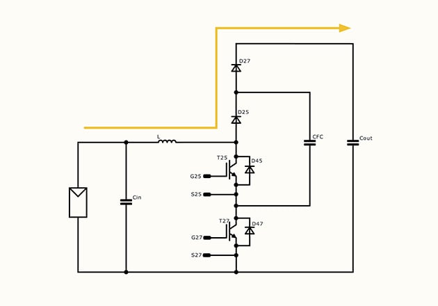
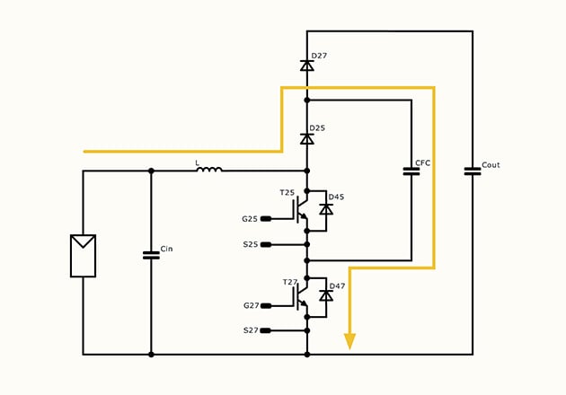
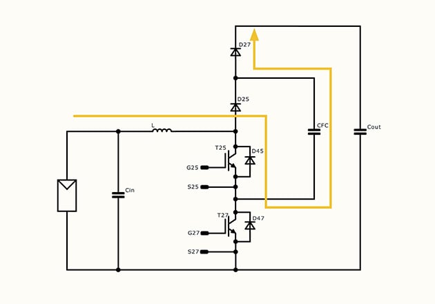
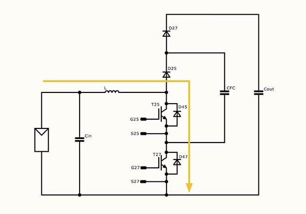
Figure 3: Operation modes of a flying-capacitor booster
| Mode | Transistors | Inductor current |
FC Voltage | DC-link voltage |
||
| T25 | T27 | D<0.5 | D>0.5 | |||
| Mode 1 | OFF | OFF | decreasing | - | - | increasing |
| Mode 2 | OFF | ON | increasing | decreasing | increasing | decreasing |
| Mode 3 | ON | OFF | increasing | decreasing | decreasing | increasing |
| Mode 4 | ON | ON | - | increasing | - | decreasing |
Table 1: Output and FC voltage states
The transfer function (y) of the flying-capacitor booster is the following:
$$y = \frac{V_{OUT}}{V_{IN}} = \frac{1}{1-D}$$
where is the duty cycle.
The used modes are dependent on the duty cycle. If, then. In this case Mode 4 is not used and the operation will be the following: … → Mode 1 → Mode 2 → Mode 1 → Mode 3 → … If > 0.5, then y > 2 , and the operation will be: … → Mode 4 → Mode 2 → Mode 4 → Mode3 → … In case of D = 0.5, y > 2 ,the operation: … → Mode 2 → Mode 3 → Mode 2 → Mode3 → …
The most commonly used operation is, when is less than 0.5.
The Operation of the Flying-Capacitor Booster
In the flying-capacitor booster topology, the two transistors have to be controlled by 180° phase shifting (Figure 4).

Figure 4: The reference and modulation signals for the PWM
This results in the case of D = 0.5, the operation modes will change between Mode 2 and Mode 3. The typical curves of the flying capacitor booster can be seen on Figure 5 in case of D = 0.2.
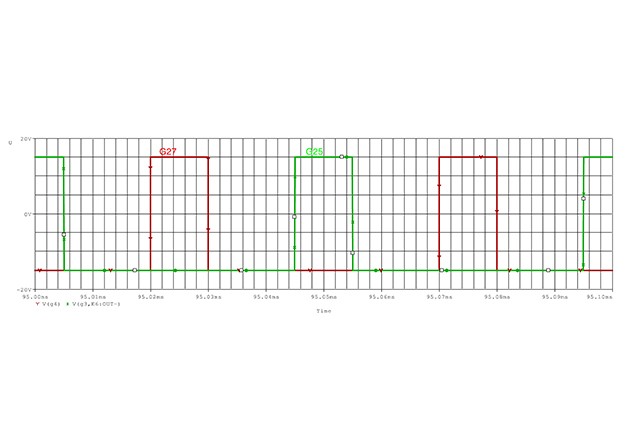
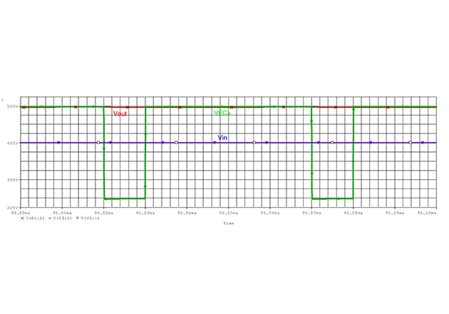
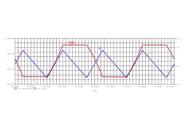
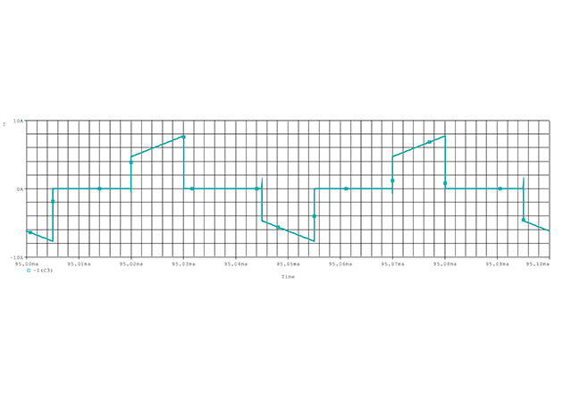
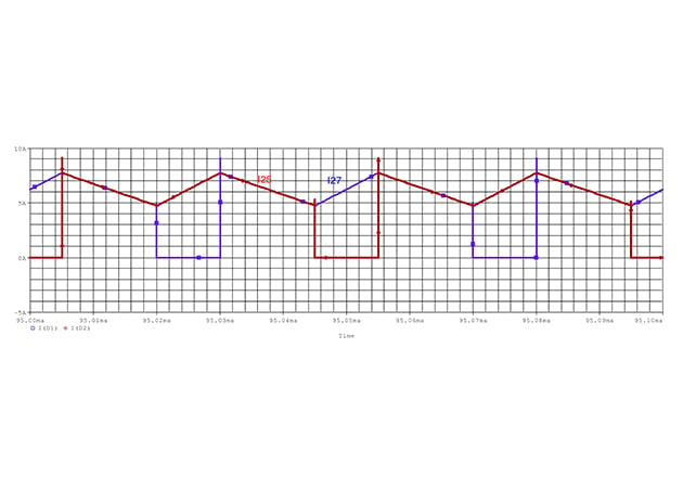
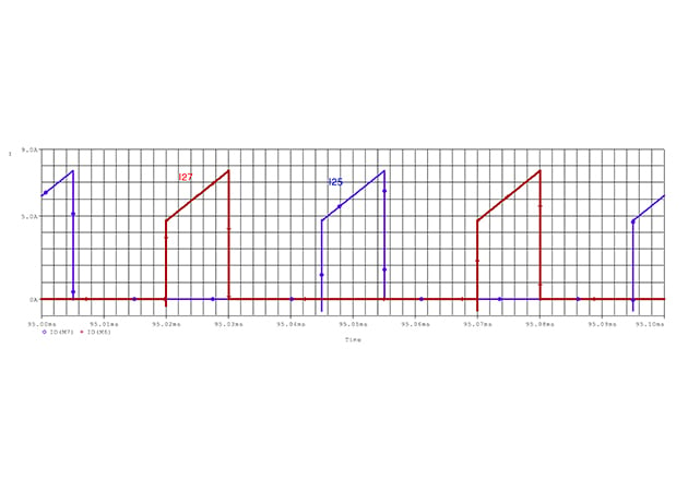
Figure 5: The typical curves a, the gate signals b, the output, the input and the FC+ voltage c, the voltage of the Flying Capacitor and the inductor current d, the Flying Capacitor current e, the currents of the diodes f, the current of the transistors
The Advantages of the Flying-Capacitor Booster
The flying-capacitor booster topology compared to the booster topology has the following advantages: • As the operation is three-leveled, the voltage stress on the semiconductor is decreased. This results in lower EMI, lower current, and voltage ripple.
The flying-capacitor booster topology compared to the symmetrical booster topology has the following advantages: • It has two-level input and output connection, while the third voltage level is synthesized by the flying-capacitor. This way the large three-level capacitors can be eliminated on the input and the output. • Only one input choke is needed.
In both cases, the input frequency is double of the switching frequency. This results in a lower input ripple current or the inductance can be decreased. Because of the double frequency, slower semiconductors can be used, which decreases the costs while the switching losses are also lower. This means for optimal behavior SiC MOSFETs are not needed, but Si IGBTs can be used.
For a more detailed comparison of the topologies and component selection, please see Vincotech’s benchmark “Boost your 1500 V string inverter”.
Conclusion
The flying-capacitor booster is a high-efficient, low cost solution for solar inverter applications. The main advantages are the frequency multiplication, the lower semiconductor voltage, the lower voltage and current ripple, the lower switching losses, and the low EMI emission, while the enormous DC-link capacitor can be also eliminated. As every other topology the flying-capacitor booster topology has some challenges also. Those will be addressed in another article.
About the Author
Viktor Antoni holds a Master's Degree and a Bachelor's Degree in Power Electronics at Obuda University. He is specialized in electronics, semiconductors and product development. Currently, he works as a Development Engineer at Vincotech since July 2017.
This article originally appeared in the Bodo’s Power Systems magazine.
Related Content