Facebook
 Google
 GitHub
 Linkedin
Isolated Flying Capacitor Multilevel Converter Modes of Operation
Isolated flying capacitor multilevel converters have various modes of operation critical to their proper working. This article explains the four different modes of operation in detail.
To catch up, read Rakesh Kumar's previous article on Isolated Flying Capacitor Multilevel Converter Basics.
The isolated flying capacitor multilevel flyback converter (FCMFC) topology employs isolated flying capacitors for high-gain DC-DC power conversion while maintaining primary-secondary isolation and enhancing the efficiency and capability of a conventional flyback transformer circuit. Three converters, one flyback as a control, a three-level FCMFC, and a four-level FCMFC, have been designed and tested to demonstrate the gain and efficiency advantages of this new topology. The FCMFC prototypes accomplish greater gains and efficiencies than a flyback design using the same commercially available transformer.
Figure 1 shows the FCMFC in its most basic form. An introduction to this converter with a focus on design and comparison has already been discussed in Part 1 of this series.
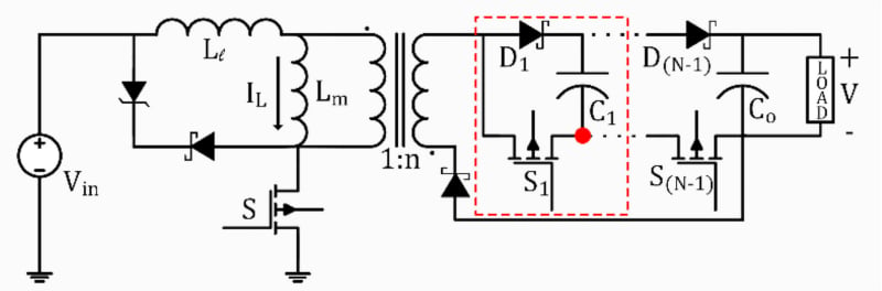
Figure 1. Flying capacitor multilevel flyback converter general form. Image used courtesy of IEEE Open Journal of Power Electronics
Converter Operation
Switching States and Voltage Gain
The FCMFC's operation is seen in Figures 2, 3, and 4. The operation would be the same for higher-level devices even though this is the simplest FCMFC, with N = 3 (or N3) voltage levels (2 capacitors: 1 flying and 1 output). With each flying capacitor, higher-level devices add two switching states: one to charge the magnetizing inductance and the other to discharge into the additional flying capacitor. The primary MOSFET controls the FCMFC's switching rate.
With S ON, the double wound inductor's magnetizing inductance will charge for DTs, as illustrated in Figure 2, where D is the input switch's S duty cycle and Ts is its switching period, which is the inverse of its switching frequency. The insertion of diode D3 at this time prevents secondary conduction through the FETs' body diodes.

Figure 2. States 1 and 3 of FCMFC operation: Charging Lm. Image used courtesy of IEEE Open Journal of Power Electronics
As seen in Figure 3, S turns OFF, S2 switches ON, and S1 turns OFF. The inductor only charges the flying capacitor C1 through D1, S2, and D3 at this point. The inductor charges up once more in the next state, which is depicted in Figure 2.
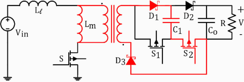
Figure 3. State 2 of FCMFC operation: Charging C1. Image used courtesy of IEEE Open Journal of Power Electronics
The output stage is shown in Figure 4, where S1 is ON, and S and S2 are OFF. Observe the current going up through the negative end of C1, through D2, and into the output capacitance in this condition. The current returns through D3. The inductor and flying capacitor work together to increase the energy of the output capacitor.
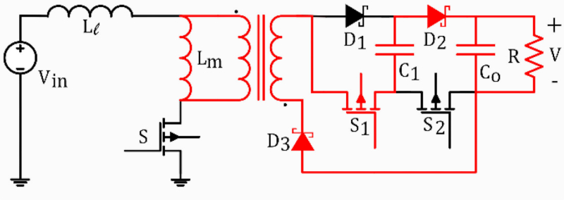
Figure 4. State 4 of FCMFC Operation Output Stage: Charging C0. Image used courtesy of IEEE Open Journal of Power Electronics
Phase-shifted pulse width modulation (PSPWM) is used to regulate the converter, as shown in Figure 5. (N-2) of the secondary switches will conduct to charge a flying capacitor stage while the primary switch is OFF.
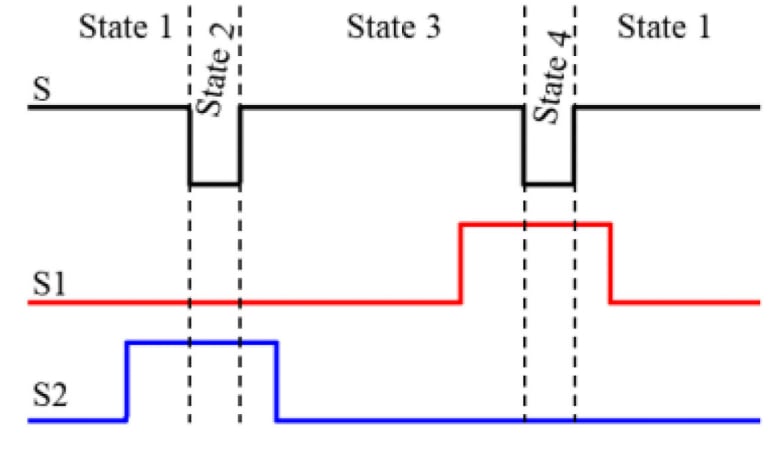
Figure 5. Phase-shifted pulse width modulation. Image used courtesy of IEEE Open Journal of Power Electronics
The voltage conversion ratio obtained using inductor volt-second balancing illustrates the energy multiplication effect that results in bigger gains. The flyback converter is the most basic FCMFC (the N2 case), and the conversion ratio for one is given by this equation. This procedure would take place for a higher N-level structure, with each flying capacitor charging the following one up until the output capacitor is charged, as depicted in Figure 4.
\[M(D)=\frac{V}{V_{in}}=\frac{n(N-1)D}{1-D}\,\,\,\,\,(1)\]
The optimal gain shown in equation (1) is plotted in Figure 6 with a transformer turns ratio of n = 5/3 for all converters. For each given duty cycle, the gain of the FCMFC is larger. On the voltage conversion ratio, the "(N-1)" term in the equation, each flying capacitor has a multiplicative impact. A flyback converter's gain is doubled with one flying capacitor, tripled with two, and so on for higher-level converters. This connection can be seen in Figure 6, which displays the voltage gain for the flyback and two FCMFC converters.
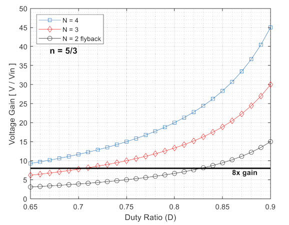
Figure 6. Ideal voltage gain vs. duty cycle for flyback and FCMFC. Image used courtesy of IEEE Open Journal of Power Electronics
However, because hardware conditions are not ideal, this ideal gain curve provides information about the absolute capabilities. The losses lower the potential gain when the flyback and FCMFC are implemented in hardware. Figure 7 displays a more precise voltage gain predictor. With analysis, these curves represent the main loss components of an FCMFC. To demonstrate what responsibility is needed for the application of this job, the flat line at eight times gain is included.
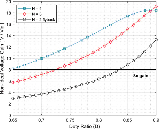
Figure 7. Non-deal voltage gain for flyback and FCMFC for 160Ω load. Image used courtesy of IEEE Open Journal of Power Electronics
As shown in Figure 6, the ideal case's necessary duty cycles are significantly lower than those in the loaded case shown in Figure 7. The N3 converter has a greater gain than the N4 converter due to conduction losses near 90% duty cycle, illustrative of the eventual tradeoff with multilayer construction. Higher N-level structures are not really always less effective, but the focus of this effort is on evidence of functioning rather than optimization. Higher-order multilevel converters with ten levels or more have been shown to be very effective.
The secondary FETs used in the FCMFC have a lowered blocking voltage rating of V/(N-1), which enables the use of lower-rated FETs with a lower on-resistance. As a result of the significant gain increase that the FCMFC experiences, all switches in this study were selected with a 100 V rating. Notably, the FCMFCs both have much higher gains than the flyback converter, even while operating under load.
Current Analysis
The average magnetizing inductor current, which was calculated using capacitor-charge balancing, is shown in equation (2). The resulting equation is identical to that of a flyback converter with an additional (N-1) term to account for flying capacitors in the numerator. While higher N-level converters can be employed with a reduced duty cycle due to the gain increase stated in the previous chapter, the magnetizing current does not directly double or triple.
For the three converters created in this paper, the average magnetizing current is determined in Figure 8 as anticipated. For N2, 3, 4 level devices, the average magnetizing currents are 2.42 A, 2.83 A, and 3.25 A, respectively. The gain increase shown reduced the input switch's duty cycle from 82.76% to 70.59% to 61.54%, respectively equation (1). The average input current of each converter is the same at 2 A in Figure 8 due to the decrease in primary side conduction.
\[I_{L}=\frac{n(N-1)V}{R(1-D)}\,\,\,\,\,(2)\]
\[\Delta i_{Lm}=\frac{V_{in}D}{2f_{s}L_{m}}\,\,\,\,\,(3)\]
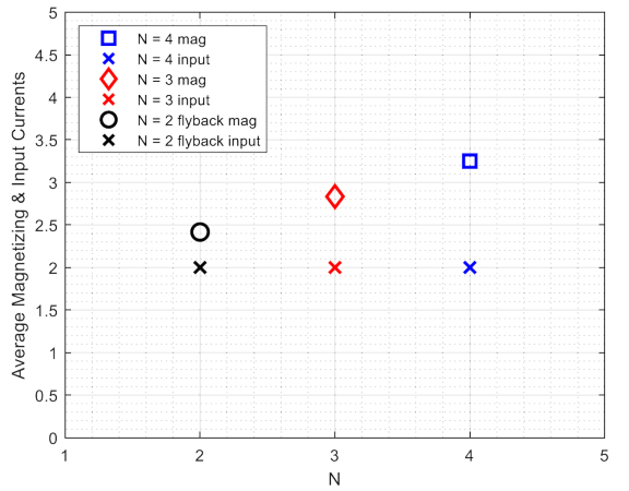
Figure 8. Magnetizing and input currents. Image used courtesy of IEEE Open Journal of Power Electronics
The magnetizing inductance Lm, the input voltage Vin, the duty cycle D, and the switching frequency fs all affect ripple current as observed from equation (3). The operating duty cycle for the desired conversion ratio is the sole variation for multilevel structures that are shown in this equation. At a given gain, a higher-level converter can operate with a reduced duty cycle, which lowers the ripple current value on the primary inductor. The computed peak current that passes through the MOSFET just before it turns OFF is shown in Figure 9. Higher-level devices have greater average magnetizing currents.
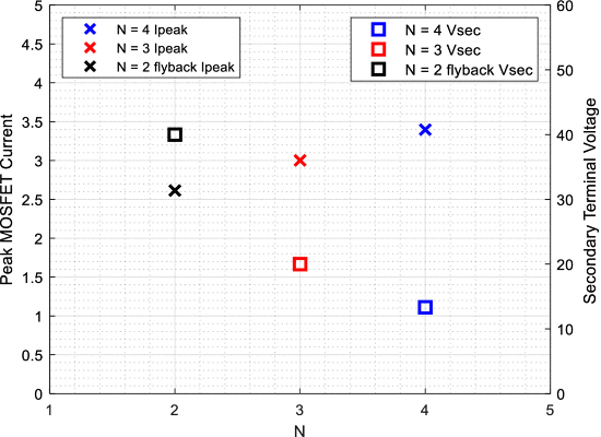
Figure 9. Peak MOSFET currents and secondary terminal voltage. Image used courtesy of IEEE Open Journal of Power Electronics
Zener Snubber Power Consumption
When the primary FET is turned off, large voltage spikes will be caused by leakage inductance on the primary winding. This is one problem with the flyback converter, but different types of snubber circuits can fix it. The most durable of these is the Zener snubber, shown in Figure 1, and is good for this exercise. From the FET's switching node to the positive input voltage node, a Schottky and a Zener diode are connected in series.
When the FET turns off, the peak current is stored in the "transformer's" leakage inductance, causing a large voltage spike across the FET. When this happens, the Zener diode will conduct at its Zener voltage, balancing the voltage at the switching node by sending the leakage current back to the source. The amount of power that this snubber circuit used is shown in equation (4).
\[P_{clamp}=\frac{1}{2}L_{lk}I_{max,S^{2}}\frac{V_{clamp}}{V_{clamp}-\frac{1}{n(N-1)}V_{out}}f_{s}\,\,\,\,\,(4)\]
One change is made to account for the FCMFC. This is the (N-1) term. This shows that when the primary FET is turned off, only a small amount of the converter's output voltage is reflected through the transformer. This is because the voltage across the flying capacitors on the secondary side of the circuit is spread out. This is shown in Figure 9, which shows the voltage at the secondary terminal as V/(N-1) for N = 2, 3, and 4.
Even though the peak FET current will be higher for higher-level converters, the reflected voltage will be much lower: 50% for an N3 converter and 33% for an N4. Using equation (4), the predicted loss in the voltage clamp snubber for these converters is much lower. When going from a flyback (N2) converter to an N3 FCMFC, the power loss drops by 67%, from 1.20 W for the flyback to 0.39 W for the N3 FCMFC because the blocking voltage is lower in the N3 FCMFC.
But notice that the power loss for an N4 device goes from 0.39 W (for an N3) to 0.40 W (for an N4). This is because the output voltage fraction is one-half instead of one-third, and the peak current goes up, as shown in Figure 9. Even though the N4 device loses 0.4 W, it still loses 66% less than the flyback converter, which loses 1.2 W. Higher-level devices lose more power through the Zener clamp snubber circuit, but it would take a 12-level device or higher to lose as much power as the flyback does.
Even though a flyback converter could use a higher turns ratio, which would reduce power loss in this snubber, this work shows how FCMFC can increase the use of off-the-shelf flyback transformers, so this is a fair comparison. The snubber could also be tuned to a higher voltage, resulting in less power loss but less protection for the primary FET, reducing its reliability.
Takeaways of Isolated Flying Capacitor Multilevel Converters Modes of Operation
This article has discussed the operation of isolated flying capacitor multilevel converters. Some of the takeaways follow.
The effects of each flying capacitor are multiplicative. With one flying capacitor, a flyback converter's gain is doubled; with two, it is tripled, and so on for higher-level converters. Because of conduction losses near 90% duty cycle, the N3 converter has a higher gain than the N4 converter, illustrating the eventual tradeoff with multilayer construction. Higher N-level structures are not always less effective; however, it has been demonstrated that higher-order multilevel converters with ten or more levels are highly successful. Higher N-level converters can be used with a lower duty cycle to increase the gain, but the magnetizing current does not double or triple. Due to the decrease in primary side conduction, the average amount of current going into each converter is the same. When the primary FET is turned OFF, the leakage inductance on the primary winding will cause large voltage spikes. This is one problem with the flyback converter, but it can be fixed using different snubber circuits.
This post is based on an IEEE Open Journal of Power Electronics research article.
Featured image used courtesy of Adobe Stock
Related Content