Facebook
 Google
 GitHub
 Linkedin
Enhancing Reliability and Compatibility With E-Mode GaNFETs
Integrating E-Mode GaNFETs with a GaN-based gate regulating circuit can significantly enhance the reliability and compatibility of gate driving for GaN switches while preserving the fast-switching properties and mitigating ringing caused by co-packaging related parasitic components.
This article is published by EEPower as part of an exclusive digital content partnership with Bodo’s Power Systems.
Integrating E-Mode GaNFETs with a GaN-based gate regulating circuit can significantly enhance the reliability and compatibility of gate driving for GaN switches while preserving the fast-switching properties and mitigating ringing caused by co-packaging related parasitic components.
Evolution and Reliability of Cascode and E-Mode GaNFETs
Cascode GaN, with a structure depicted in Figure 1 (a), combines a low-voltage normally-off silicon MOSFET and a high-voltage normally-on GaN HEMT in a cascode configuration. The combination effectively results in an enhancement-mode behavior, and this technology has been commercially available since the early 2010s. The silicon MOSFET, with a common gate threshold voltage of 4 V, simplifies the gate drive requirements compared to native GaN solutions, as those Cascode GaNs can typically be driven with standard silicon gate drivers. In addition, the hybrid nature of a silicon MOSFET can enhance reliability. Silicon’s known characteristics and behavior can be leveraged to protect the more sensitive gate of GaN HEMT, reducing the risk of failure due to high voltage spikes or improper gate voltage.
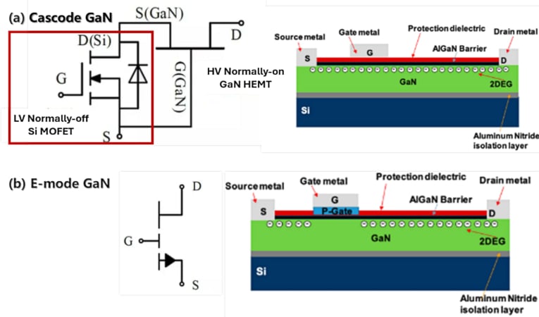
Figure 1. Schematic comparison between (a) Cascode GaN and (b) E-mode P-gate GaN HEMT. Image used courtesy of Bodo’s Power Systems [PDF]
However, the extra silicon MOSFET between the gate and source of GaN HEMT will considerably increase the effective input capacitance of the Cascode GaN device, which largely sacrifices fast-switching characteristics, one of the most outstanding advantages compared to SiC MOSFETs. What’s worse, the series connection of silicon MOSFET and D-mode GaN for co-packaging will lead to additional parasitic inductance that causes more ringing and overshoots in the switching waveforms, affecting overall performance and raising concerns about electromagnetic interference (EMI).
E-mode GaNFETs, as shown in Figure 1 (b), use a p-type GaN gate structure to provide a positive threshold voltage, making the device normally off inherently in a single-chip solution. This is crucial for power applications where fail-safe operation is necessary. E-mode GaNFET typically exhibits very low gate charge and capacitances without any extra components, resulting in faster switching speeds and reduced switching losses. They are highly efficient in applications requiring high-frequency operation.
Nevertheless, the p-type GaN gate provides a typical lower gate threshold voltage of 1.4 V, which would cause accidental device turn-on and system failure due to noise or gate voltage fluctuations. Furthermore, the typical driving range is -10 V to 7 V, incompatible with the driving voltages for most other power devices, which require 12-18 V, making it difficult to switch to GaN HEMTs from other power switches. Lastly, as the p-type GaN gate is not quite mature and more vulnerable, there are concerns about its long-term reliability and threshold voltage stability.
All-GaN-IC Solution: A Leap in Gate Threshold Voltage and Driving Range
GaNPower International has innovated an All-GaN-IC method that boosts the gate threshold voltage from 1.4 V to an impressive 3.5-4.0 V, with an extended driving range up to ±20 V. A proprietary GaN-based gate regulating circuit has been monolithically integrated with the power GaNFETs in a single chip. This innovation, depicted in Figure 2 (a), aligns the new E-Mode GaN with the pin-outs, threshold voltage, driving range of silicon and SiC MOSFETs, earning it the nickname ‘pin-to-pin’ (P2P) for its exceptional compatibility. The P2P technology combines the advantages of Cascode GaN and E-mode GaN. It aims to achieve a more reliable gate driving without largely compromising the fast-switching benefits of GaN power switches.
According to the LTSpice simulated results shown in Figure 2 (b), the gate threshold voltage of the P2P GaN switch has been increased to around 4 V, and its gate voltage has been properly clamped below 7 V by All-GaN-IC with 0-20 V PWM input.
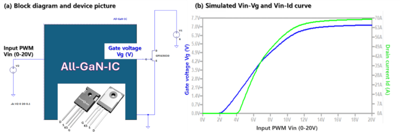
Figure 2. (a) Block diagram and (b) simulated verification of a gate regulator circuit monolithically integrated with a main E-mode p-gate GaNFETs. Image used courtesy of Bodo’s Power Systems [PDF]
Room temperature experimental static IdVg measurement results, presented in Figure 3, also verify the enhancement of gate threshold voltage (3.6 V) for the P2P GaN, compared to normal E-mode GaN without the GaN-based gate regulating circuit.

Figure 3. Comparison of Ids-Vgs measurement between 650V 30A E-mode GaN HEMT (a) without and (b) with a monolithically integrated gate regulator circuit (i.e., P2P technology). Image used courtesy of Bodo’s Power Systems [PDF]
Demonstrating Superior Switching Performance
A double pulse testing platform with a customized air-core 128 μH load inductor, a freewheeling SiC diode, and a reliable voltage clamp circuit for accurate dynamic Rdson measurement has been built for the burst-mode switching evaluation of the P2P GaN.
With 12 V PWM input and 900 V bus voltage, all the switching waveforms (Vgs, Vds, and Ids), as shown in Figure 4, are clean without considerable ringing or overshoots. In addition, the dynamic Rdson is also within a reasonable range of up to 33 A (its current ratings) drain current under room temperature, which can be observed from the clamped Vds waveforms. Another double pulse test conducted at similar loading conditions under 125°C shows comparable switching waveforms demonstrating good GaN-based gate regulating circuit thermal stability.
A 100 KHz half-bridge Buck testing platform with a high saturation toroidal power inductor and a constant 40 ohm high power resistor load was built for the continuous hard-switched evaluation of the P2P GaN. Two GP65R45T4 devices with suitable heat sinks were installed on the main test board, and proper fan cooling was used during the tests.
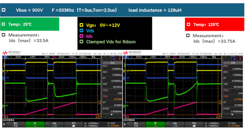
Figure 4. The results of double pulse testing (DPT) at 33 A drain current and 900 V bus voltage demonstrate good switching performance at both (a) 25°C and (b) 125°C. Image used courtesy of Bodo’s Power Systems [PDF]
According to the efficiency reports shown in Figure 5 (a), with 12 V PWM input and 200-550 V bus voltage, the P2P GaN-based buck converter achieved a peak efficiency of 97.42% and a maximum power output of 3.7 kW. Figure 5 (b) demonstrated good continuous switching waveforms without substantial ringing and overshooting at the peak efficiency with 450 V bus voltage.
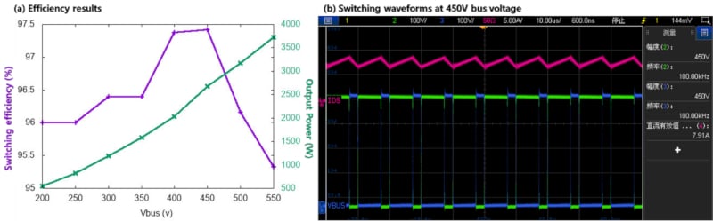
Figure 5. (a) Switching efficiency and (b) switching waveforms of an air-cooled half-bridge Buck converter, where two GaNPower P2P GaN HEMTs (GP65R45T4) were under continuous hardswitched tests. Image used courtesy of Bodo’s Power Systems [PDF]
More rigorous reliability testing on a large scale of GP65R45T4 samples is in progress to ensure the P2P GaNs are reliable and optimized in practical industry applications.
This article originally appeared in Bodo’s Power Systems [PDF] magazine. Featured image used courtesy of Adobe Stock.