Facebook
 Google
 GitHub
 Linkedin
EiceDRIVER and CoolMOS CFD2 Join for High Efficiency in Refrigeration
This article discusses the benefits and advantages of CoolMOS CFD2 in terms of efficiency in motor drive applications and gives recommended layouts.
Home appliances that run 24 hours a day, 7 days a week, have many high-efficiency requirements, therefore the use of MOSFETs is preferred over IGBTs. Provided that the modern MOSFET technologies based on the superjunction principle are nevertheless challenging to control in motor drive applications, in which this article describes the basic considerations for a successful gate drive circuit design and explains the benefits of combining EiceDRIVER ICs and CoolMOS CFD2.
Commutation Cell Analysis of BLDC Drives
A half-bridge cell, as depicted in Figure 1, is enough to study the switching behavior of all FETs. S1 and S2 are switching in a buck configuration; S4 is turned ON permanently to provide the return current path. S1 is the active switch and the inductor current ramps up when S1 is turned on. S2 is the rectifier switch — its body diode carries the inductor current when S1 is OFF and the inductor current ramps down. This mode of operation takes place for one-third of the motor’s cycle, then the same operation moves to the next half-bridge. The switch-mode operation of MOSFET causes high dv/dt and di/dt.
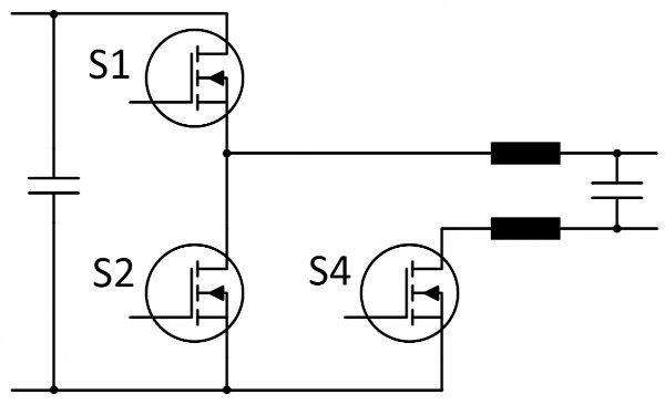
Figure 1: Switching cell

Figure 2: Parasitic elements of the MOSFET, package, layout, and driver
Risks of High dv/dt
A major risk of high dv/dt is shoot through that S1 is turned ON and the resulting dv/dt across S2 couples to its gate and a voltage spike appears. If the coupling spike is high enough to reach the FET’s gate threshold voltage, then both FETs in the bridge will be on for a short period of time, causing failures also in components such as shunt resistors or electrolytic capacitors.
Another risk is gate oscillation, which can be triggered at turn-ON. High di/dt causes a voltage drop across the source inductance of the FET’s package and layout. This voltage forms negative feedback to the driving voltage, causing the FET’s gate to resonate as depicted in Figure 3.
Additionally, high dv/dt at turn-OFF can couple to the gate through the drain-gate capacitance, causing oscillations.
These concerns are related to the FET’s parameters, package, and layout parasitics as shown in Figure 2. These have to be addressed by the gate driver design.
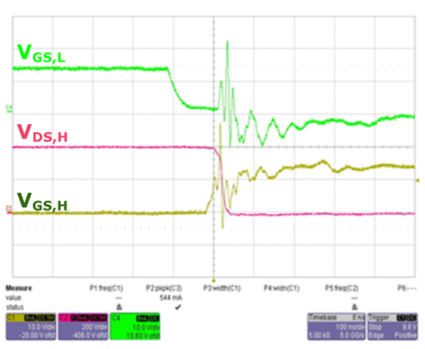
Figure 3: Strong oscillations during the turn-ON of a MOSFET
Origin of dv/dt and Application Effects
The dv/dt takes place during the charging period of the reverse capacitance Crss, as seen in Figure 2 represented by the charge Qgd. Hence, the Crss value and the charging current level are two factors that affect dv/dt. Higher gate resistance Rg value means charging Crss with a lower current, which extends the Miller plateau time and reduces dv/dt.
The current change rate dIrec/dt during reverse recovery of the MOSFET´s body diode generates a voltage across the parasitic source inductance which is a positive feedback to the driving voltage. It causes a faster charging of Crss and higher dv/dt. Diodes with snappy recovery behavior lead to higher dv/dt. Moreover, the snappiness increases the voltage overshoot on S2, caused by the loop inductance.
During turn-OFF, the non-linear capacitance Coss in Super-Junction FETs like CoolMOSTM CFD2 and the low Coss values at high voltages Vds lead to increased dv/dt. This provides a low switching loss and fast voltage transition but also requires careful layout and gate driver design techniques taking the higher dv/dt into consideration.
Proposed Gate Circuit Design for CoolMOSTM CFD2
Figure 4 shows a proposed schematic using CoolMOSTM IPD65R420CFD. Most notable is the capacitor Cds=0.47nF added to each bridge´s switch node to limit and linearize the dv/dt. This is the most reliable approach to prevent shoot-through and resonance problems. In motor drive applications, the typical switching frequency is low, therefore the added capacitor Cds only has a minor impact on the switching losses. Other driving parameters are chosen considering:
- Ron=1000 Ω: slower turn ON, longer plateau, reduced dv/dt.
- Roff=0 Ω: Lower impedance to GND when turned OFF, lower voltage coupling spike.
- Cgs=0.47nF: reduced Crss/Ciss ratio, reduced drain-gate, or Miller coupling gain.
- Cds=0.47nF: controlled/linearized dv/dt at turn ON, this has the benefit of removing gate oscillation and reduce EMI.
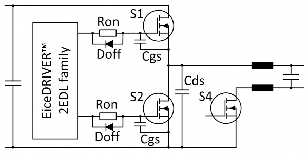
Figure 4: Proposed gate circuit schematic for CoolMOSTM CFD2 using EiceDRIVER 2EDL family
The circuit is operated by a 2EDL05N06PF EiceDRIVER IC. Based on Infineon´s SOI technology, it provides excellent robustness against negative transient voltages [3]. The excellent properties of the integrated bootstrap diode support the requirements of high power density and cost-performance ratio.
Layout Recommendations
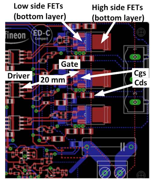
Figure 5: Example of a layout with minimized stray inductances by means of a double-side assembly
Figure 5 depicts a layout with minimized stray inductance due to the short distance between the high side source terminal and the low side drain terminal. The low side transistors on the bottom layer are shifted to the left side with respect to the high side transistors on the top layer. This leads to a thermal decoupling of both transistors. Furthermore, the low side transistors move even closer to the respective gate resistors.
The shift also allows that the drain terminals of the low side transistors move directly underneath the source terminals so that an appropriate number of vias provides a close connection to the high side source terminals. Hence, the loop inductance is minimized. A double-sided assembly can be avoided when placing the low side transistors appropriately onto the top layer. This, of course, will lead to higher area consumption.
In general, these layout guidelines are recommended for reducing noise and resonance in the gate drive loop:
- Gate driver as close as possible to the gate.
- Minimum external capacitance gate to drain.
- Slow down dv/dt by properly choosing the gate resistor Rg.
- Separate power ground from gate driver ground.
- Rg as close as possible to the gate pin.
- Use thick trace between the gate driver and gate.
The physical proximity of the gate resistors to the gate terminals as simple gate design in combination with the reduced stray inductances leads to improved performance and excellent switching behavior of the CoolMOS™ transistors. A turn-ON waveform of the proposed driving circuit design is given in Figure 6. It shows a clean gate signal free of oscillations and the drain-source voltage slowly ramping down to 0V during the Miller plateau region, too.
![Turn-ON waveforms at DC-link voltage VDC = 320 V and load current IL = 2.5 A. VDS (red, 50 V/div), IL (green, 1 A/div), VGS (blue, 10 V/div), PWM (yellow, 5 V/div), time scale 1 µs/div]](https://eepower.com/uploads/thumbnails/957-4844-infineon.jpg)
Figure 6: Turn-ON waveforms at DC-link voltage VDC = 320 V and load current IL = 2.5 A. VDS (red, 50 V/div), IL (green, 1 A/div), VGS (blue, 10 V/div), PWM (yellow, 5 V/div), time scale 1 µs/div]
The same behavior can be expected for the other two switching bridges given that the layout and driving circuit is the same.
Higher Efficiency with CoolMOSTM CFD2
CoolMOSTM CFD2 offers efficiency benefits in motor drive applications. The proposed gate drive circuit design using the EiceDRIVER 2EDL family ensures an oscillation-free switching. This leads to the conclusion that CoolMOSTM CFD2 can be efficiently and reliably operated in drives systems. Additionally, Infineon´s silicon on insulator (SOI) technology, which is used for the 2EDL family, provides a high robustness with respect to dv/dt in motor drive applications and excellent controllability of CoolMOS CFD2.
About the Author
Wolfgang Frank is the Principal Engineer for Product Definition and Concept of gate driver ICs at Infineon Technologies, Augsburg, Germany. Earning his degree in Power Engineering from Technical University, Munich, he has worked in power engineering for over 20 years.
References
- R. Mente, F. Di Domenico, M.A. Kutschak, A. Steiner: CoolMOS™ CFD2 first 650 V rated super junction MOSFET with fast body diode suitable for resonant topologies, Application Note, Infineon Technologies, February 2011.
- W. Choi, D. Son, M. Hallenberger S. Young: Driving and Layout Requirements for Fast Switching MOSFETs, Fairchild Semiconductor Power Seminar 2010-2011, Fairchild, 2011.
- J. Song, W. Frank: Robustness of level shifter gate driver ICs concerning negative gate voltages; Proceedings of PCIM 2015, Nuremberg, Germany, 2015.
This article originally appeared in the Bodo’s Power Systems magazine.