Facebook
 Google
 GitHub
 Linkedin
Reduce Size and Increase Efficiency with GaN-based LLC Solutions
GaN High Electron Mobility Transistors (GaN HEMT) have a lower driving loss and shorter deadtime circuit benefits due to significantly reduced gate
GaN High Electron Mobility Transistors (GaN HEMT) have a lower driving loss and shorter deadtime circuit benefits due to significantly reduced gate charge (Qg) and output capacitance (Coss) compared to silicon MOSFETs. Therefore, GaN HEMTs show significant advantages over silicon MOSFETs in high-frequency soft-switching resonant topologies such as an LLC resonant converter. With increased switching frequency (fsw), the transformer core size can be reduced. Furthermore, a 3-D PCB structure is employed to increase the power density. A 190-Watt, 400V-19V GaN Systems E-HEMT-based LLC DC-DC resonant converter is carefully designed, and the transformer is optimized for high-end adapter applications operating above 600kHz. The converter shows a complete design with a power density over 63W/inch3, including the 400V bus capacitor, with a peak efficiency of 96%.
High power density is one key motivation for GaN HEMTs to be widely used in low power consumer applications such as laptop adapters, flat screen TVs, and all-in-one desktop computers.
The LLC resonant convert topology is effective in improving efficiency, especially for high-input voltage applications where the switching loss is more dominant than the conduction loss. The series and parallel inductors are often integrated into the transformer using the leakage and the magnetizing inductance, thus reducing the component count. The purpose of this article is to demonstrate a high-power density and high-efficiency DC-DC LLC solution using GaN HEMTs.

Table 1. QG and COSS Comparison.
The Capability of GaN HEMTs Operating in High-Frequency, Soft-Switching LLC Applications
Compared to silicon MOSFETs, GaN HEMTs feature significantly reduced gate charge (Qg) and output capacitance (Coss), resulting in lower driving loss and shorter turning-on/off periods. Therefore, GaN HEMTs show significant advantages over silicon MOSFETs in high-frequency soft-switching resonant topology such as the LLC resonant converter.
In order to take a closer look at the potential advantages of GaN in high-frequency soft-switching resonant converters, we have to compare the key parameters of GaN HEMTs to those of the conventional Si MOSFETs. As an example, GaN Systems’ GS55504B is selected to be compared to the active Si MOSFETs (IPx65R110CFD and IPP60R105CFD7) because they have comparable RDS(ON) values. The following table shows the comparison of the key parameters: VDS, RDS (ON), QG, CO (ER) and CO (TR).

Figure 1. Qg Comparison

Figure 2. Gate-driver loss comparison
A. The Qg Advantage of GaN
As shown in Figure 1, the GS55504B features significantly reduced gate charge (Qg) compared to both the IPx65R110CFD and IPP60R105CFD7, resulting in a lower driving loss. Figure 2 shows the comparison of gate-driver loss at different switching frequencies. The loss difference between the two devices increases dramatically with the increase of the switching frequency, demonstrating the advantage of GaN HEMTs working at the high switching frequency.

Figure 3. Coss Comparison

Figure 4. Coss energy comparison

Figure 5. Coss charging time comparison at the turn-off.
B. The Coss Advantage of GaN
Coss of a Si MOSFET is highly nonlinear at low voltage. The Coss values of a GaN HEMT features significantly reduced output capacitance (Coss) and Coss energy, resulting in shorter turning-on/off period, as shown in Figure 5. This characteristic allows the shorter deadtime and higher switching frequency operation to be achieved.
C. The GaN advantage in LLC resonant converter
The schematic of the GaN-based half bridge LLC converter is plotted in Figure 6.

Figure 6. GaN-based half-bridge LLC converter.
For the LLC resonant converter working in the below-resonance region and at the resonance point, primary side half-bridge switches, S1 and S2, always safely turn on without incurring switching loss (Zero-voltage Switching). The total loss resulting from the power switches is composed of three parts: 1) driving loss (decided by Qg), 2) conduction loss (decided by RDS(ON)) and 3) switching off loss (decided by Coss). It has been analyzed that the GS55504B has the all three mentioned advantages over the Si MOSFETs when applied to the high-frequency soft-switching frequency LLC converters.
The design specification of the LLC converter is shown in Table 2, which is very popular in two-stage adapter applications. The LLC tank is designed, and the parameters are listed in Table 3.

Table 2: Design Specifications

Table 3: LLC Resonant Tank Parameters
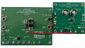
3D PCB Structure Solution for High-Power-Density LLC Resonant Converter
A. 3-D Structure Concept
In order to push the power density of the GaN HEMTs based LLC prototype, the "3-D PCB" concept is also utilized, where all the active switches, power diodes, and MCU are assembled on the PCB daughter cards.
B. Implementation
The whole LLC system design is composed of the following four parts:
PCB Board 1
Primary side half-bridge daughter card with two GaN HEMTs (GS66504B) and bootstrap driving circuitry (32mm (L) × 19mm (W)). Since GS66504B are a bottom-side-cooling device, one 17mm × 17mm square shape heatsink is connected to the bottom side of PCB to cool the two GaN HEMTs.

Figure 7. Primary side half bridge daughter card PCB layout (top) and pictures (bottom).
PCB Board 2
Primary side digital controller with peripheral circuits (26mm (L) × 20mm (W)). The topology employs a digital control solution integrating an output voltage regulation, OVP, and OCP function into one low-cost MCU (DSPIC33FJ06GS202A from Microchip).

Figure 8. Primary side digital controller daughter card PCB layout (top) and pictures (bottom).
PCB Board 3
Secondary side synchronized rectifier daughter card (20mm (L) × 17mm (W)). All the components are soldered on only the top side. One 20mm × 20mm square shape heatsink is connected to the bottom side of PCB to cool the four Synchronized Rectifier MOSFETs (2 × 2 paralleled MOSFETs).

Figure 9. Secondary side synchronized rectifier daughter card PCB layout (left) and pictures (right).
PCB Board 4
Motherboard with input capacitor, output filter, and integrated transformer (69mm (L) × 34mm (W)) is shown in Figure 10. Three slots are provided on the motherboard for PCB board #1, PCB board #2, and PCB board #3 to be inserted.

Figure 10. Designed GaN-based LLC Resonant Converter Prototype.
C. LLC prototype and its power density
The finished prototype and its dimension are shown in Figure 11. All the heatsinks are connected to the bottom side of the daughter cards, which is effective for the bottom-side cooling devices, such as GaN HEMT, GS66504B, on the PCB board #1 and secondary side synchronized rectifiers PCB board #3.

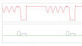
The key waveforms of designed high-frequency LLC converter working at half load and full load are shown in Figure 11 and Figure 12.

Figure 11. The key experimental waveforms of the proposed high-power-density GaN HEMT LLC converter when Vin=400V, Vout=19V, Io=5A Po=95W, Fs=623kHz (50% load).
The efficiency at different loads is tested and shown in Figure 13, the power loss from the auxiliary winding is not included. The peak efficiency has achieved 96.1% at 95W (50% load) while the efficiency at 190W (100% load) is 95.6%.

Figure 12. The efficiency performance at different load when Vin=400V, Vo=19V, Io=1A (19W) to 10A (190W).
The efficiency at different loads is tested and shown in Figure 13, the power loss from the auxiliary winding is not included. The peak efficiency has achieved 96.1% at 95W (50% load) while the efficiency at 190W (100% load) is 95.6%.
GaN HEMTs Offer Higher Switching Frequency
The GaN HEMTs features a superior figure of merit (low Qg, RDS(ON) and COSS) which enables the resonant converter such as the analyzed LLC allowing operating at a high switching frequency over 600kHz. The smaller core using high-frequency magnetic materials can then be employed to increase the power density. Furthermore, with the help of 3-D PCB structure as well as the combined digital control solution, the prototype shows a complete 400V DC-19VDC design with a power density of 63W/inch3 while its peak efficiency has achieved 96.1%.
About the Author
Yajie Qiu is a Senior Power Electronics Applications Engineer at GaN Systems Inc. He got master's degree of power electronics at Anhui University of Technology and having gained a PhD of electrical engineering/power electronics at Queen's University. He has experience in commercial product designing on medium-power offline LED lights, circuit designing and debugging in a switched mode power supply (SMPS) including voltage regulators, LLC resonant converters, and PFC converters.
Related Content