Facebook
 Google
 GitHub
 Linkedin
Driving SiC MOSFETs & IGBTs With Current Source Gate Driver
This article outlines how ROHM’s new current source gate driver – the BM60059FV-C – offers a possibility of reducing switching losses by up to 26% while operating at a limited dv/dt.
When a parameter is changed, it often entails a number of other changes. Finding the perfect design is therefore often very difficult. If a power semiconductor is controlled in such a way that it switches faster, switching losses are reduced and resulting in better system efficiency. On the other hand, it is precisely this high switching speed that can have a negative impact on the service life of other components such as motor insulation and can cause EMI issues. Constant Current Drive Technology can reduce the switching losses with a limited dv/dt.
On the other hand, it is precisely this high switching speed that can have a negative impact on the service life of other components such as motor insulation and can cause EMI issues. With its new gate driver BM60059FV-C, ROHM offers a possibility of reducing switching losses by up to 26% operating at a limited dv/dt.
Current source drivers (CSD) and voltage source drivers (VSD):
Figure 1 shows block diagrams of gate driver BM61M41RFV-C, a conventional voltage source driver versus BM60059FV-C, a current source driver. The ideal turn-on characteristic of an IGBT and the corresponding gate current for individual type of driver are also shown. In this whole article only the turn on characteristics will be considered.

(A) Image used courtesy of Bodo’s Power Systems

(B) Image used courtesy of Bodo’s Power Systems

(C) Image used courtesy of Bodo’s Power Systems

(D) Image used courtesy of Bodo’s Power Systems
Figure 1. Typical turn on characteristics of an IGBT using voltage source driver BM61M41RFV-C (A and C) and current source driver BM60059FV-C (B and D). Image used courtesy of Bodo’s Power Systems
The well-known turn-on characteristics are split into six intervals (T0 – T6). Neglecting the parasitics, internal gate resistance of the power device and internal RDS(on) of the push-pull stage MOSFETs, the peak gate current at the instant T0 is given by,
$${I_{G\_Peak}}=\frac{VCCC2}{R_{g}}$$
Equation 1.
where VCC2 is the supply voltage of the gate driver with respect to the driver ground GND2, Rg is the external gate resistance. In the time T0-T2 the input capacitance (CGE and CGC) of the IGBT is getting charged. The cumulative gate current during this interval can be expressed as,
$${I_{Gate}}(t)=\frac{VCC2-{V_{GEO}}}{{R_{g}}}.{e^{-(t-T0)/({R_{g}}.\big({C_{GE}}+{C_{GC}}\big))}}$$
Equation 2.
During the interval T2 to T4, in the so-called Miller plateau, the gate voltage remains constant and so does the gate current. This current can be expressed as,
$${I_{Gate(T2-T4)}}=\frac{VCC2-V_{GE}(Miller)}{R_g}$$
Equation 3.
During T4 to T5, VCE has already fallen to a very low value. This will make the gate current decay with a time constant given by,
$${{^{\tau}}_{T4-T5}}=R_{g}\,.\,(C_{GE}+C_{GC})$$
Equation 4.
The gate voltage further increases to VGE+ with the same time constant and the turn on process is complete. A more detailed explanation and equations can be found in [1].
On the other hand, for a current source driver, the gate current from the instant T0 to T5 remains constant and is expressed with a simple equation,
$$I_{G-CSD=}\frac{V_{OUTREF}}{R_{OUTREF}}$$
Equation 5.
where VOUTREF is a fixed internal reference voltage of the gate driver BM60059FV-C and is typically 2V and ROUTREF is the external resistance that needs to be adjusted as per the switching speed needs.

Figure 2. Gate current and gate voltage measurement with a constant current source driver BM60059 and a 1200V IGBT at no load for different ROUTREF values. Image used courtesy of Bodo’s Power Systems
Figure 2 shows the gate current and gate voltage waveforms of three different ROUTREF settings while driving a 1200V IGBT with the driver BM60059FV-C. A constant gate output current in each of the cases can be clearly observed.
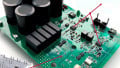
The region of interest while comparing a current source driver and a voltage source driver is the period T2-T3 where the dv/dt is determined by the gate current during the Miller plateau. In this region only the gate-collector capacitance is being charged, whose value is strongly dependent on the voltage. At a high collector-emitter voltage, the Miller capacitance is low and upon turn-on, as the voltage starts to fall its value increases. The Miller plateau is also load dependent and especially at high load currents, its voltage VGE(Miller) is higher [1]. From equation 3, it is evident that at higher Miller plateau voltages, the gate current is lower. Thus, by using a voltage source driver one can expect the turn-on dv/dt to be steadily decreasing with increasing load, leading to higher turn-on losses. On the other hand, a current source driver with its ability to maintain a constant gate current output, a constant dv/dt can be achieved over the complete load range. This translates into a reduction of turn-on losses at high load current, when using current source drivers instead of voltage source drivers. To verify the benefits and expectations of a constant current source driver, a test board was developed where discrete IGBTs and SiC-MOSFETs were tested. A standard voltage source driver was also implemented on another board, see Figure 3.


Figure 3. Half bridge test board with voltage source driver (top) and current source driver (bottom). Image used courtesy of Bodo’s Power Systems
| Power device | Gate drive voltage | Conditions | Type of gate driving |
| 1200V, 100A, TO-247-4L IGBT |
15V – Turn on 0V – Turn off |
VDC = 600V Tamb = 25°C |
VSD (ROHM Driver: BM61M41RFV) |
| 1200V, 100A, TO-247-4L IGBT |
15V – Turn on 0V – Turn off |
VDC = 600V Tamb = 25°C |
CSD (ROHM Driver: BM60059FV) |
| 1200V, 55A, TO-247-4L, 40mΩ SiC MOS |
18V – Turn on 0V – Turn off |
VDC = 600V Tamb = 25°C |
VSD (ROHM Driver: BM61M41RFV) |
| 1200V, 55A, TO-247-4L, 40mΩ SiC MOS |
18V – Turn on 0V – Turn off |
VDC = 600V Tamb = 25°C |
CSD (ROHM Driver: BM60059FV) |
Table 1. Tests and conditions. Courtesy of Bodo’s Power Systems
Experimental Results:
Both the current source driver and the conventional voltage source driver boards were evaluated using double pulse tests. A 1200V, 100A discrete IGBT and a 1200V, 55A, 40mΩ SiC-MOSFET were evaluated. Both devices are housed in a TO-247-4L package, which includes a driver emitter/source pin. Only unipolar gate drive was used for both cases: 15V/0V for the IGBT and 18V/0V for the SiCMOSFET. Table 1 shows the list of tests that were performed with the corresponding conditions. Voltage source drive and current source drive will be hereafter mentioned as VSD and CSD respectively.
For all the tests an active Miller clamping function was used. For the analysis only the turn-on losses were considered. The power devices were evaluated for different load conditions and different switching speeds. Figure 4 shows the dv/dt comparison of voltage source driving and current source driving of IGBT and SiC MOSFET for different gate resistances. The gate resistance in a VSD is represented as Rg and the equivalent resistance to control the gate current for a CSD is given as ROUTREF.
It is quite evident from the figure that at slower switching speeds (dv/dt < 10V/ns), a CSD maintains a constant dv/dt over the complete load range for both SiC MOSFET and IGBT, which is not possible with a conventional driver. For normal to high switching speeds, CSD and VSD behave similarly. This means that only applications where a low dv/dt is mandatory will benefit from CSD.

(1) Image used courtesy of Bodo’s Power Systems

(2) Image used courtesy of Bodo’s Power Systems

(3) Image used courtesy of Bodo’s Power Systems

(4) Image used courtesy of Bodo’s Power Systems
Figure 4. Measurement results dv/dt during turn on CSD with IGBT (1), VSD with IGBT (2), CSD with SiC (3), VSD with SiC (4). Image used courtesy of Bodo’s Power Systems
Use case of current source drivers:
In applications such as motor drives, it is common to limit the dv/dt of the switching power devices to 5V/ns. A higher dv/dt can eventually damage the motor windings and lead to premature aging. For industrial motor drives, IGBT-based inverters are the norm and the benefits of current source driving of IGBT has been discussed in [2]. It has also been reported that using SiC-MOSFETs with limited dv/dt using conventional gate drivers can result in much better efficiency compared to an IGBT-based motor drive [3]. The benefit of using SiC-MOSFETs in drives application can be further exploited using CSD.

(A) Image used courtesy of Bodo’s Power Systems

(B) Image used courtesy of Bodo’s Power Systems
Figure 5. Comparison of turn on losses with maximum dv/dt limited to 5V/ns (A: IGBT, B: SiC-MOSFET). Image used courtesy of Bodo’s Power Systems
Hence, four possible solutions with a maximum dv/dt of 5V/ns are analyzed:
1. Voltage source driving of IGBT
2. Voltage source driving of SiC-MOSFET
3. Current source driving of IGBT
4. Current source driving of SiC-MOSFET
In the case of the 1200V, 100A discrete IGBT with VSD a gate resistance of 22Ω is needed to limit the maximum dv/dt to 5V/ns. With CSD, a gate current setting of 290mA (ROUTREF value of 6.8 Ω) is needed. For a 1200V, 55A SiC-MOSFET using a VSD, a gate resistance of 27Ω is needed to limit the dv/dt to 5V/ns and with current source driver, gate current setting of 290mA (ROUTREF value of 6.8 Ω) is needed. Figure 5 shows the turn on energy loss comparison of CSD and VSD of SiC and IGBT where the maximum dv/dt at any load is limited to approximately 5V/ns.
For an IGBT-based solution, the turn-on losses using both CSD and VSD start with an approximately similar value at low load (0.5mJ) but at high load there is a 22% loss reduction by using a CSD. Likewise for a SiC based solution, both the CSD and VSD start with turnon losses of 0.25mJ but at high load there is a 26% loss reduction by using CSD. Summing up, the turn-on losses can be reduced using a CSD mainly at high load conditions due to their ability to maintain a constant dv/dt at any load. Clearly this is an advtantage when using CSD in slow switching applications.
Current Source Gate Driver Conclusion
In conventional gate drivers where gate resistors are used to limit the switching speeds of the power semiconductors, the dv/dt upon commutation is strongly load current dependent. On the other hand, a constant dv/dt can be realized over a complete load range with a current source driver. ROHM’s new isolated gate driver BM60059FV-C offers this feature upon turn-on. Experimental verifications show that at high load range and slow switching speeds (<5V/ ns), current source driving of SiC-MOSFETs or IGBTs reduces turnon losses by up to 26% in comparison to the conventional method. In applications such as motor drives where the dv/dt is commonly limited to 5V/ns, current source drivers increase the efficiency and offer a promising solution.
This article originally appeared in Bodo’s Power Systems magazine and was co-authored by V. Thayumanasamy, F. Filsecker, C. Felgemacher, J. Kleinpaß, and K. Lenz of ROHM Semiconductor.