Facebook
 Google
 GitHub
 Linkedin
Digital Control in High Power AC-DC Converters with PFC
This article discusses on microcontroller based digital control architecture of high power AC-DC converters featuring power factor correction (PFC).
Design of High Power(1 kW and above) AC-DC converters featuring Power Factor Correction (PFC) is challenging task with issues like ripple currents in input power line, inrush current at start-up, switching high currents at inductive load, Electro Magnetic Interference (EMI), current balancing in polyphase topology, fast reaction on load change, efficient protection, and many others. Microcontroller (MCU) based Digital Control architecture along with high power discrete components from IXYS allow solve most of the critical issues on the way to build high power AC-DC converters with PFC.
Digital control has significant advantages compared with traditional hardware implementation of high power converters:
- Programmable algorithm overlooking all aspects of conversion including inrush control, current balancing, over-current/over/voltage protection, and so on;
- Easy adjustment to the load variations by maintaining high efficiency in wide load range;
- Capability to accommodate different user requirements with few corrections in software and unaltered hardware;
- Replicable design that does not require sample to sample adjustment to get expected result
High Power Digitally Controlled Two-phase AC-DC Converter with PFC
To graphically demonstrate all these advantages, High Power Digitally Controlled Two-phase AC-DC Converter with PFC (Converter) was designed. It utilizes two Zilog’s 8-bit Z8F6481 MCUs and IXYS hardware components including novel X/X2 class trench MOSFETs.
Converter was tested with up to 1000 W and higher load. The load limitation was imposed by input power line rating and inductor’s capability. This design can be extended to substantially higher conversion power, if needed.
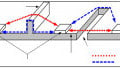
Figure 1 illustrates a functional diagram of the Converter. Power factor correction is implemented using two-phase interleaved boost type conversion architecture. For Phase 1, it is executed with inductor L1, switching device T1, and diode D1. For Phase 2, boost conversion is accomplished with L2, T2, and D2. High Power factor is achieved by adjusting a peak current value with respect to rectified input voltage, which is used as a reference, Vin. Peak currents are captured with sense resistors Rs1 and Rs2 and amplified to the range of 2 V.
Due to high current values, the inrush current at start-up is digitally controlled and the bulk capacitor’s C pre-charge is performed in pulse mode by switching device T3, along with inductors L1 and L2. The digital inrush current control concept utilized here was published in [1].
Current sense resistor Rs3 is used to monitor bulk capacitor’s C current and the load current. It is also responsible for the overload protection functionality. Load current is sensed during zero crossing of the input AC voltage, when the inductor is discharged and capacitor C is the only source of energy provided to the load. At this moment, the capacitor’s current is equal to the load current. This allows connecting the load to the rectifier’s ground directly and eliminating the current sensing resistor in between.
The overload protection is continuously active with the comparator set to monitor the load current. In an event of overload, the comparator shuts down conversion. The MCU can be programmed to wait for a predetermined period of time and attempts to restart the converter. Additional programmable features include the number of restarts and the period between attempts.

Figure 1: Functional Diagram for MCU controlled AC-DC Converter with PFC
Overvoltage protection is based on measuring output voltage during the AC line zero-crossing time frame and comparing it to the programmable overvoltage reference. If overvoltage occurs, the device is shut down to prevent high output voltage in case of low load.
Principle of Operation
The following operational principles are considered for this design:
- Peak inductor current modulation was chosen over other PFC topologies aiming at high power conversion.
- Quasi-resonant mode is used as a version of critical conduction mode, allowing inductor voltage to drop to its lowest value in resonant process with strain capacitance after the inductor is discharged into a load.
- The second conversion phase is set as slave with respect to the first “master” phase.
- The balance of phase currents is performed using hardware and software.
- Low power consumption (less than half of peak power) forces the second phase into sleep mode.
- Pulse density modulation is used in addition to amplitude modulation to maintain efficiency of conversion at low loads.
- An active snubber is used to reduce stray oscillation after the inductor is discharged into the load.
- A Look-Up Table (LUT) is used to simplify calculations performed by the 8-bit MCU.
- Prediction control is performed with LUT assistance. Prediction is set to about 95% of expected output parameters.
- Digital feedback is used to keep output parameters in the predetermined range.
Peak Inductor Current Modulation ‒ The Peak inductor current modulation architecture allows average line current to copy a form of the AC line input voltage. In this design, a rectified and scaled input sine wave is used as a reference. It applies to the analog input of the DAC, while digital DAC’s input is used to set the amplitude of the inductor current in respect to output power required. A signal from DAC’s output provides reference voltage for peak current modulation.
Switching operations are paused near the AC input voltage zero-crossing area to improve converter’s efficiency by avoiding switching at low input voltages when the voltage cannot be boosted to the required output level.
Figure 2 demonstrates inductors current/voltage waveforms at AC input of 120 V RMS and~700 W load. The peak inductor current amplitude is 12 A and peak voltage is 400 V. The bottom of the scope snapshot is a zoom-in of the top portion of the area between two vertical white lines.
Quasi-resonant Mode ‒ The MCU allows maintain quasi-resonant mode by tracking the point of the inductor’s discharge and providing the necessary delay before turning the inductor’s current on again. The delay value may have some variance, because the inductor voltage has a dull bottom plateau, but inductor current changes smoothly as shown in Figure 3.
Quasi-resonant mode of operation is maintained at high power until power consumption approaches half of peak power, after which pulse density modulation is used to keep high efficiency of conversion.

Figure 2: General Waveforms of Two-phase MCU-controlled PFC Converter
Legend:
Blue and Magenta – First and second inductor voltages. Scale -100V/div
Green and Yellow – First and second inductor currents. Scale – 5A/div
Lower half of the picture is a zoom of the top portion at the position of
vertical white lines

Figure 3: Quasi-resonant Mode Waveforms
Legend:
Magenta – First inductor voltage;
Green – First inductor charging current;
Yellow – Gate voltage for first phase MOSFET


Figure 4: Inductor Voltage with Snubber Active (top) and Snubber Disabled (bottom)
Legend:
Magenta –inductor voltage;
Green – inductor charging current;
Yellow – Gate voltage for MOSFET;
Blue – power line current
Lower half of the picture is a zoom of the top portion at the position of vertical white lines
Second Conversion Phase is synchronized with the master phase. Synchronization is implemented by delaying start of the second phase conversion cycle with respect to the first phase timing.
Balance of Phase Currents to reduce ripples in the input power line is achieved by varying delay time of the start of second phase conversion. MCU adjusts delay time for every next conversion cycle based on previous conversion cycle timing. Peak inductor current for the second phase is controlled with the same reference that is used for the primary phase that allows keep them identical.
Low Power mode is determined as less than half of the nominal load consumption. Power consumption is monitored by measuring load current during AC input voltage zero crossing, where conversion is halted, but output voltage VOUT is maintained in the specified range. If load current drops below half of the maximum rated value, the second phase conversion is halted.
Pulse Density Modulation is used to further reduce generated power, when power consumption falls more than half of the rated power.
Active Snubber is used at low power consumption and low pulse density during the time frame from inductor’s discharge to the start of the next conversion cycle. Snubber timing is set by the MCU. An illustration of active snubber performance is shown in Figure 4.

Figure 5: Two-dimensional Representation of R_Load in LUT


Figure 6: DAC Control Sets for Two-phase (Top) and Single-phase (Bottom) Conversion Modes
Look-Up-Table (LUT) simplifies MCU operations to speed up the algorithm. The data for LUT is converted to an 8-bit representation. The main LUT data contains load impedance, which is estimated by measuring output voltage VOUT and load current iLoad. Load impedance is more informative because it is estimated not only in steady-state, but also in transition modes, when VOUT and iLoad are not settled yet. For simplicity of MCU operation, the load impedance is calculated as resistive parameter R_Load.
The R_Load = f (iLoad, VOUT) graph is represented in Figure 5, where iLoad is the horizontal axis. The axis values are in 8-bit representation for R_Load, 7 bit for VOUT, and 6 bit for iLoad. At low iLoad values, R_Load is limited, and VOUT is controlled with feedback. If there is no load VOUT is maintained by burst of conversion pulses or may be programmed to go in shut down mode.
The LUT based algorithm is also used in prediction control.
Prediction Control sets initial values for peak inductor current DACdata supplied to DAC digital input and for delay of the next conversion pulse (indicated as Delay) to modulate pulse density.
Empirically obtained DAC data is a convoluted result of the influence of input voltage VIN and load power consumption POUT. VIN influences converted power as inverse square function 1/VIN^2. The input voltage range is set from 105 V to 140 V and scaled down to 1.72 V - 2.4 V for ADC measurement as shown in Figure 6. The power load is set from 60 W to 1070 W. The actual power values used are shown in the colored legends in the top right corner of Figure 6.
Prediction LUT
The prediction LUT is constructed as a two-dimensional LUT representing DACdata = f (VIN, R_Load). Prediction LUT is shown in Figure 7 in actual 8-bit data values along the X-axis for VIN and Y-axis for R_Load. Prediction control is designed to accommodate for about 95 % of control values for DAC and Delay needed to maintain output power. The Feedback Loop provides then precise correction of DAC data to keep output voltage within 1% range.
Another prediction LUT is used for delay prediction as a function of R_Load, Delay = f (R_Load). The Delay is zero at low R_Load (high power), then Delay steadily increases with the reduction of power consumption (increase of R_Load) as shown in Figure 8.
Digital Feedback ‒ Digital feedback finalizes the conversion algorithm as it modifies DACdata loaded as prediction value with feedback control value. The overall algorithm of feedback and its addition to DACprediction value is shown in Figure 9. The feedback control value is calculated once per AC half period at zero crossing, to be loaded into registers as a conversion time for following half of the sine wave period. The calculations are performed at 16-bit resolution in order to have smooth DAC control, which is of 12-bit resolution. The feedback data consist of two terms: integral term iTerm and differential term dTerm. The differential term acts as leading control to increase the stability of the control loop while reducing the settling time. KD and KI constants are used to balance the ratio between terms, while KER sets the feedback gain.

Figure 7: Prediction of DAC Control as a Function of VIN and R_Load

Figure 8: Prediction of Delay as a Function of R_Load

Figure 9: Feedback and Prediction Control Algorithm

Figure 10: Scope snapshots depicting feedback reaction on a load boost from 60% to 100%
Legend:
Blue – First inductor current. Scale -5A/div
Green – Load Current measured with amplifier. Scale – 0.8A/div
Magenta – output voltage. Scale – 100V/div
Lower half of the picture is a zoom of the top portion at the position of vertical white lines
The feedback loop control is set over prediction control to increase the accuracy of the output voltage. Prediction data and feedback data are calculated around zero crossing and applied for the next half-wave of the input voltage. At the time around zero crossing, there is no active conversion and the only source of load current is a bulk capacitor. The current value is measured by MCU and is used then as an index for retrieving data from LUT.
Output voltage undershoots and overshoots at the time of rising and falling of load current as it is shown on Figure 10. Over/undershoots of the output voltage are at 7% range with a duration of 100 ms. Output voltage stays steady after transitions.
Hardware Implementation
Discussed Converter’s hardware implementation is shown in Figure 10. It consists of an MCU Module and a Main Power Board. The MCU Module is implemented as an add-on device. It contains connectors for MCU programming, because the MCU should be programmed before powering the entire system.
The Main Power Board is a two-layer surface-mount board that provides easy access to test points. The Converter may be powered from a 50 Hz or a 60 Hz 105 V to 140 V AC source. Auxiliary power supply of +3.3 V for the MCU and 12 V for the gate drivers on the Main Power Board requires.


Figure 11: MCU Module (Top) and Main Power Board with MCU Module (Bottom)
Testing Converter
The AC power line current was measured with a current probe at 20MHz bandwidth. The scope snapshot of the power line current is depicted in Figure 12. The total AC power line current value is the sum of currents into two conversion phases involved, which results in AC power line current hovering over the peaks of the single inductor current. Use of EMI filter centered at conversion frequency allows smooth current ripples. Overshoots at the beginning and end of the conversion period are caused by EMI filter. The Converter offer following features:
- Conversion power, maximum: 1.06 kW @120V power line
- Input Voltage: 105 ‒ 140 V AC 50/60 Hz
- Output Voltage: 400 V ± 2%, programmable
- Output Current: 2.65A @400V
- Output Voltage Ripples: <6% at full load
- Input Current Ripples: <2%
- Load Variation Range: >10x
- Device Conversion Frequency: 100‒120 kHz at high power
- Programmable Overload, Overvoltage, and Brownout Protection
- Digital Inrush Current Control
- Soft Start Mode
- Power Good Status

Figure 12: Scope snapshots depicting power line current along with inductor current and voltage
Legend:
Yellow – Power line Current. Scale – 5A/div,
Green – Inductor current Scale -5A/div,
Blue – Inductor voltage. Scale – 100V/div
Lower half of the picture is a zoom of the top portion at the position of vertical white lines.
The current is shown only for one conversion phase.


Figure 13: Efficiency of Converter in 10X load range (Top) and zoom of upper area (Bottom)
Legend:
Red – Converter efficiency at 130V power line;
Black – Converter efficiency at 110V power line;
Horizontal axis – power, Watt
Efficiency of the Converter was measured at 110V and 130V power line voltages. For given high power and relatively low power line voltage, efficiency is quite reasonable. It is expected to reach efficiency to about 98% going ahead with extending input voltage range to 220V -240V due to increasing output power at the same conducting losses. That can be seen from Figure 13 where the increase of efficiency by 1% is resulted in by changing input voltage from 110V to 130V. At high power, two conversion phases are active. Efficiency slightly reduces with decreasing load until one of the active phases becomes disabled. Then the trend repeats for single conversion phase at low power. Converter’s efficiency is maintained within +/-1% variations at 10X load variation.
Discussions
Digital control in power conversion provides flexibility in contemplating the overall algorithm, designing dedicated features, and tailoring the design to customer needs. Use of MCU allows achieved high efficiency in a wide range of loads and input voltages, while maintaining stable output voltage. Efficiency is achieved due to optimization between peak inductor (switching MOSFET) current and conversion pulse density. Power consumption is monitored by MCU, which disables the second phase to reduce switching losses.
Inductor current balancing for two-phase interleaved conversion is controlled by MCU maintaining identical peak current value and calculating start position for second phase current thus reaching ultimate current balancing state. Prediction of conversion parameters speeds up settling of optimal peak current values and pulse density by programming conversion pulses delay for the next AC line half sine-wave based on previous one. At 95% of predicted value to required one, the task for feedback control is greatly simplified leading to faster settling and high precision of the output voltage.
Use of fast MOSFETs and diodes based on latest X/X2 class designs from IXYS allows achieve fast switching at high current leading to increased efficiency. Peak current modulation controlled by MCU allows modulate current from power line to be close to reference with precision of processing capabilities of MCU hence introduced harmonics are at low level.
About the Authors
Anatoliy Tsyrganovich, PhD, is working at IXYS Corporation as a Systems Architect. He is responsible for developing novel concepts, algorithms, models, and devices to highlight capabilities of company products; MCU based digital power control allows implement flexible, efficient algorithms with fast reaction to the load variations. Analyzing market trends and technology problems to contemplate new products and requirements for current product enhancements. He earned both his Master's degree and PhD in Electrical Engineering, Major in Digital Signal Processing and Image Enhancement at All-Union Correspondence Power Institute of Electrical Communication from Moscow, Russia and Minsk Division, Belarus, Russia respectively.
Leonid Neyman, Senior Application Manager at IXYS, holds a Master’s degree in electromechanical engineering from Saint Petersburg State University of Aerospace Instrumentation, Russia, and Ph.D. degree in electronics engineering from Saint Petersburg State Electrotechnical University, Russia. His main engineering field is mixed analog/digital design, and is the author of 28 patents.
Abdus Sattar works as the Director of Engineering at IXYS Corporation. He is responsible for leading the vision to drive product roadmap, product planning, new product development, and solve complex customer issues with strategic tradeoffs between cost, features, and performance; align priorities with corporate objectives while optimizing resources by balancing large-scale projects with cross-functional resources to meet deadlines; and act as a strategic innovation leader to CEO and CTO and deployed product line strategy to bring new ideas for evaluation and potential rollout and implementation. He is a graduate of Bachelor's and Master's degree in Electrical Engineering at Rajshahi University of Engineering & Technology and South Dakota State University respectively. He then earned his PhD in Electrical Engineering at Santa Clara University, California, USA.
References
- Anatoliy Tsyrganovich, Leonid Neyman, and Abdus Sattar, IXYS Corporation “Limit Inrush Control in AC-DC Power Supplies and Rectifiers” Electronic Design, September, 2015
This article originally appeared in the Bodo’s Power Systems magazine.