Facebook
 Google
 GitHub
 Linkedin
Solving Industry Inrush Current Problem with IXYS Digital Power Controller
This article illustrates advantages of digital power control that overcomes many disadvantages of the inrush current problems with power devices.
Inrush current creates problems with power devices and with interference of those devices with power line, and circuit breakers. It also affects the reliability of the power system due to overstress caused by instantaneous but huge surge in initial current at power-up. There are known solution to limit inrush current in AC-DC devices [1], [2] requiring lossy components like resistor or conventional NTC resistor with transistor on relay shunt to attenuate inrush current. Our approach written in this article has two objectives: first, to illustrate advantages of digital control that overcomes many of the disadvantages of the existing technology and second, to raise interests in digital control of the high power converters, stimulating development of its next generation.
Raising interest in digital control, which overcomes many of the disadvantages of the existing technology to limit inrush current at high power converters, initiated this design. It combines IXYS digital power control technology with Zilog’s 8-bit Z8F3281 MCU capabilities to illustrate a unique approach to control inrush current in high power AC-DC rectifiers and AC-DC converters with capacitive load by limit-ing capacitor pre-charge current to a predetermined value at each half sine-wave cycle. Capacitor charge is spread over a number of cycles until capacitor is charged proportionally to a peak value of AC voltage source.
IXYS digital inrush current controller features programmable overload protection and “Power Good” status signal. It is not sensitive to power outage, brownout and ambient temperature variations. It can operate with input voltage range from 80V to 240V AC and load current up to 3A. Entire operation process and essential values are fully programmable. The controller may be programmed to 50 Hz, 60 Hz or any other line input frequency operation.
Time-Dependent Pulse Train
The circuit schematic is presented in Figure 1 in which the key concept is to provide charge to bulk capacitor in equal increments. Capacitor is charged according to time-dependent pulse train. The pulses are designed in a way to provide substantially equal voltage increment applied to the capacitor to keep peak of charging current about the same value at each cycle. Number of cycles depends on capacitor value and charge current. For a given capacitor value, which is selected depending on desired ripples amplitude, the charge current is a function of number of pulses and its timing position with respect to rectified sine wave.
We can consider N cycles for inrush control operation and then split the normalized amplitude of half-rectified sine wave to N segments with increment of 1/N as shown on Figure 2. During Cycle 1, Sw1 is on (conducting) from the time stamp t1 to T thus allowing the capacitor C charge to the voltage proportional to normalized value 1/N. The charging current does not rise instantly because it is a current in serial LC resonant circuit. That shapes the current waveform to the resonant one. The current is rising until capacitor voltage reaches input voltage excluding voltage dropouts.
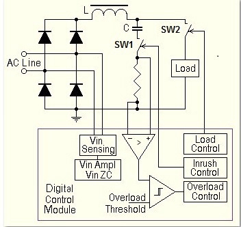
Figure 1: Circuit Schematic for Digital Inrush Controller

Figure 2: Digital Inrush Control timing
Then current continue its resonant behavior because Sw1 is still conducting. No further oscillation occurs because input voltage drops below the voltage on the capacitor, and then Sw1 is off (not conducting). Capacitor remains pre-charged to the voltage proportional to 1/N. In Cycle 2, capacitor C is pre-charged by another voltage increment 1/N in the process similar to Cycle 1. Capacitor C is charged N cycles to the voltage value proportional to the input line voltage.
Principle of Operation
Another variable to control inrush current is LC time constant. Capacitor C value depends on desired ripple value. After selecting the capacitor C value, the designer can decrease peak inrush current by increasing inductance L. If there are physical limits to L value, the number of cycles N should be used to set the required peak current.
Turn ON time for Switch Sw1 should be defined for each active cycle. For cycle 1 in Figure 2, the delay from the zero-crossing point (point 0 in Figure 2) to the beginning of turning Sw1 on, t1, is denoted as T_off. The time between t1 and T, an active time to keep Sw1 on is denoted as T_on, and the period or cycle duration is denoted as T.
Active time T_on for each occurrence i is defined as geometrical transform:
The period T is measured by MCU at initialization. Values of T_on are determined by (1) and stored in memory. Values of T_off are derived by firmware according to following expression:
Figure 3 conceptually illustrates algorithm behavior as it is executed in MCU Z8F3281. Timing counter (red line) corresponds to time at any given moment of discrete-time base provided by an internal clock. The counter first counts till T_off value represented by green line. When counter reaches T_off value it initiates T_on pulse (yellow line) which continues according to counter reaches T_on value (magenta line). Blue line (rectified power line voltage) is shown for reference. Magen- ta represents actual T_on time value in µs for each cycle, and yellow is T_on pulse positioned relatively to rectified power line voltage.
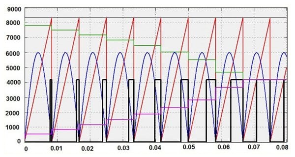
Figure 3: An illustration of T_on timing generation. Legend: Blue – rectified power line voltage, Red – full cycle period timing counter, Black – driver to Sw1, Green – time OFF to Sw1, Magenta – Time ON to Sw1.
An illustration of timing position and amplitude of capacitor C current (green line) with respect to T_on pulses are depicted in Figure 4. It is noted that Inrush Controller generates a single current pulse during a cycle. Because after the capacitor C charge is completed, the input voltage drops below the capacitor voltage and the input power line is isolated from the rest of the circuitry by the diode bridge circuit. Inductor discharges into capacitor C, then switch Sw1 is OFF (not conducting) at the end of the cycle. The algorithm is based on reactive power transfer, hence, losses are limited mostly to those on strain resistance.
Switch Sw2 is optional. It is implemented in this design to connect load after capacitors is charged completely, as well as add an Overload Protection functionality. Sw2 is activated at zero crossing on the next cycle after capacitor is pre-charged. On simulation in Figure 4, it occurs at time stamp 0.066ms, when capacitor current shows up as negative because current is sourced from the capacitor. The Sw2 activation can be programmed to any other timestamp point depending on customer requirements.
Also, MCU generates Power Good signal, which can be delayed in respect to Sw2 on state, to let load stabilize before some other functions are executed. The overload threshold is programmable as well, and it is set to 3.5A in current design.
Overload Protection
Overload Protection is a valuable feature to protect a device from been destroyed in case of overload or continuous overload. If overload is detected by a comparator, then the MCU disconnects the load by turning OFF Sw2 and shuts down Sw1. Overload protection can be programmed for two modes of operation: (i) immediately shut down the device and wait for user interference and (ii) allow device restart predetermined number of times.
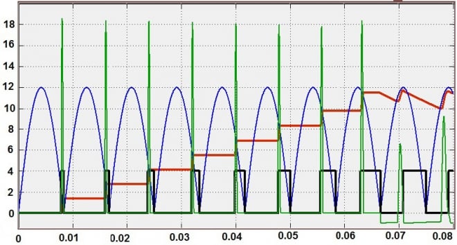
Figure 4: Capacitor C pre-charging. Legend: Blue – rectified power line voltage, Red – voltage on Capacitor C in respect to common Ground, Black – drive signal to Sw1, Green – Capacitor current. (Not to scale)
After initial pre-charging and connecting the load, the MCU may be reconfigured for other power managing tasks. For example, it can perform power factor correction (PFC) control and keep track records on device performance, overload conditions, power outages, power brownouts, etc. Based on collected information, the MCU is able to inform user on reliability state of the device and supply statistic information of a system performance.
IXYS Digital Inrush Controller
IXYS Digital Inrush Controller which consists of an MCU Module and a Main Power Board is shown in Figure 5 (a) and (b). The detail circuit schematics are included in Figure 6. The MCU Module is implemented as an add-on device. The module comprises connector for MCU programming. The MCU should be programmed before powering the entire system. The MCU Module is powered by auxiliary power supply +3.3V for MCU and 12V for gate driver applied to the connector J4 on the Main Power Board.

Figure 5: (a) MCU module and (b) Main Power Board with MCU module
The Main Power Board is a two-layer PCB with diode bridge, MOS-FETs Q1 (Sw1), and Q2 (Sw2), mounted on small heat sinks. Power dissipated on these heat sinks is less than 5 W at 375 W output power. This board may be powered from 50 or 60 Hz AC source.
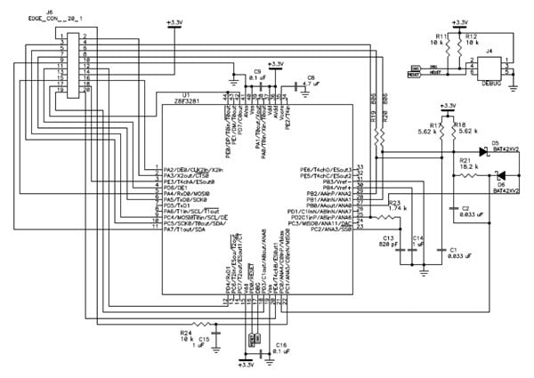
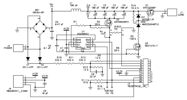
Figure 6: Detail schematic diagrams (a) MCU Module and (b) Main Power Board
Testing Digital Inrush Controller
Performance of the design has been verified by several bench tests. A scope snapshot of the test result is shown in Figure 7. Testing confirmed that the inrush current is limited to predefined value and performance of the limiter is quite close to simulation results. The amplitude of the inrush current is limited to the value equal to the input current at maximum load to minimize the negative impact on AC line, as well as limit electromagnetic interference (EMI), by selecting of number of inrush current pulses equal 16 and inductor 100 μH. The AC input line is connected through an isolation transformer. The load is connected at rectified voltage zero-crossing one-half wave after the output capacitor is completely charged (see red line in Figure 7).
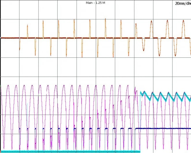
Figure 7: Scope snapshot of the Digital Inrush Current Control. Legend: Orange – power line current (10A/div), Cyan – Load voltage (50V/div), Magenta – rectified input voltage (50V/div), Blue –Sw1 drive signal.
Figure 7 depicts Sw1 gate drive pulse (blue line) and rectified voltage (magenta line) at the input of the device. Rectified voltage slightly drops after load is connected due to the limited output power of the isolation transformer used during the test. Orange line depicts line current and cyan line depicts the load voltage. The system is verified to provide 2.5A output current at full load or normal operation. Inrush current is limited to 10A.
Measured efficiency of the inrush control path is 99.5%. The device is capable of working in a wide range of input voltage: 80V to 240V. Tested power line frequency range was 50 Hz and 60 Hz. Dedicated control pulse train was developed for each power line frequency. To apply higher power line voltage, a longer control pulse train is needed in the implementation. For instance, increasing the AC line voltage from 110V to 220V requires a double pre-charging time than that of 110V to have the same peak inrush current.
Overload protection is based on continuous monitoring of the dynamic current from bulk capacitor, In case of an overload condition, the cur-rent drawn from capacitor C instantly increases and the comparator inside the MCU initiates the system overload mode. Overload current threshold, number of overload instances, and the period between overload events are programmable. The system response is being verified successfully by testing an overload condition. The load has been increased to draw an output current of 3.5A which triggers an overload protection. The system is also tested with continuous overload that results in multiple attempts to restart the system with immediate interruption. Power Good status is not present in overload conditions. This overload protection is not sensitive to power interrup-tions, brownout, and temperature variations.
Conclusions
IXYS Digital Inrush Controller offers flexibility in implementing a unique control algorithm that aids in efficient power system. It achieves a high level of efficiency, increased stability, and reliable performance across a wide range of loads. Because of an innova-tive current measurement algorithm, it allows common input and load grounds. Users can optimize the device for a wide range of input voltages and frequencies. This design provides instant over-current protection, followed by an intervention by the MCU for corrective actions.
About the Author
Anatoliy Tsyrganovich received his PhD at University of Electrical Communications Engineering, Moscow, Russia. He worked as fellow, systems architect at IXYS Corporation that gained a worldwide reputation as a premier power semiconductor manufacturer. Its diversified product base of specialized power semiconductors, integrated circuits and RF power is utilized by more than 2500 customers worldwide, ranging across industrial, transportation, telecommunications, computer, medical, consumer and clean tech markets. Learn more about IXYS’ 30-year history, its founder Dr. Nathan Zommer, its divisions and current growth.
Leonid Neyman worked as a senior manager, application at IXYS Corporation, a company that gained a worldwide reputation as a premier power semiconductor manufacturer. Its diversified product base of specialized power semiconductors, integrated circuits and RF power is utilized by more than 2500 customers worldwide, ranging across industrial, transportation, telecommunications, computer, medical, consumer and clean tech markets. Learn more about IXYS’ 30-year history, its founder Dr. Nathan Zommer, its divisions and current growth.
Abdus Sattar received his Doctor of Philosophy (Ph.D.) in the Field of Electrical Engineering focused on power semiconductor devices. He worked as a Director Of Engineering at IXYS Corporation that gained a worldwide reputation as a premier power semiconductor manufacturer. Its diversified product base of specialized power semiconductors, integrated circuits and RF power is utilized by more than 2500 customers worldwide, ranging across industrial, transportation, telecommunications, computer, medical, consumer and clean tech markets. Learn more about IXYS’ 30-year history, its founder Dr. Nathan Zommer, its divisions and current growth.
References
- Randhir Singh Malik, William Hemena, Circuit for limiting inrush current to a power source, US6445165 B1, Sep 3, 2002. [2] Michael Allen, Understanding power supplies and inrush current, Electronic Products, March 206, pp. 64, 65.