Facebook
 Google
 GitHub
 Linkedin
Achieving 99% PFC Efficiency with ICERGi Gate Drives and Digital Control Technologies
This article demonstrates low-cost, extremely-high-efficiency, and Si-based implementation of PFC stages enabled by innovative ICERGi gate drive and digital control technologies.
Power factor correction (“PFC”) functionality is a fundamental building block in all midrange power supplies for electronic equipment. ICERGi's work primarily relates to power levels from about 300W – below which efficiency rarely gets commercially rewarded – up to 3kW, which corresponds approximately to the limit for practical single-phase operation.
Achieving 99% efficiency for PFC front-end stages has been a domain of wide bandgap (WBG) devices due to reverse recovery challenges associated with high-voltage (> 500V) silicon super junction MOSFETs. Such limitation, however, doesn’t hold true for low voltage (< 150V) silicon variants deployed in multi-level bridgeless totem pole PFC which has been researched and developed by ICERGi. This article demonstrates low-cost, extremely-high-efficiency, and Si-based implementation of PFC stages enabled by innovative ICERGi gate drive and digital control technologies.
Totem Pole Topology for PFC
Recent commentary has pointed out the relevance of the totem-pole topology for power factor correction. In a topology context, this is a very simple circuit, as shown in Figure 1. It also has the advantage of using a single PFC inductor as compared with the dual semi-bridge approach, which requires a dual inductor.

Figure 1. “Basic” totem pole circuit implementation
The active switches are stacked as shown – which immediately rules out silicon super junction technology due to the Qrr reverse recovery challenge – and the extreme shoot-through current and associated losses that are a consequence of the high Qrr values. This is the main challenge to its usage and may explain the historical preference for conventional “bridged” boost solutions in spite of the power loss due to the extra diode drop in these “bridged” types.
The logical approach is to use devices with low Qrr as the active switches – and hence the usage of GaN or SiC (collectively “wide bandgap”, or “WBG”) types. Getting soft switching in a PFC context is difficult – given the wide range of operating conditions – and hence hard switching is the norm. The low capacitance of WBG devices assists here, in limiting losses under hard switching, albeit with challenges in dVdt and dIdt management. Getting 99% efficiency with such device types is no longer seen as a “rare” accomplishment. Design concerns here revolve around the newness of WBG devices, the lack of dual sources and the very high cost of devices.
99% Efficiency with Silicon
Getting 99%+ efficiency performance with low-cost, mature, multi-sourced silicon switch technology is the desire, rather than having a sole reliance on WBG devices. And it IS possible, and well proven in multiple designs. A topology set that can use silicon VERY well (performance AND cost) in a totem-pole Power Factor Corrector using multilevel approaches. Multilevel approaches have been used for some time at higher voltage and power levels, and are well proven with a considerable body of accumulated industry experience and analysis captured in academic publications. Usage of multilevel technologies in a totem-pole power-factor correction stage is as in Figure 2.

Figure 2. Usage of multilevel technology in totem-pole power factor correction
Multilevel usage has many additional attractive characteristics including:
- Inherent frequency multiplication – where each cell switches at a low frequency with the effective frequency being a multiple of the cell frequency
- Low-voltage switching – where each cell is switched at low voltage. Alongside the low switching frequency property, as cited above, this can result in very efficient operation with low switching losses
- Inherently lower dVdt and dIdt – of value in limiting EMI/EMC effects
- The topology operates with phase cancellation, implying reduced voltage applied to the PFC inductor for reduced time. As inductor size tends to be a function of applied volt-seconds, there is the opportunity for making this key component small and neat as compared with the traditional “large and bulky” part.
Multilevel conversion also uses mid-voltage FETs – so a universal-line power factor correction stage with a nominal output voltage of ~400V, can use for example 2x300V, 3x200V, 4x150V or 6x100V types. Such FET types are readily available from multiple suppliers.
Most characteristics of lower-voltage FETs are also considerably “nicer” than those of their 600V high- voltage cousins. Specifically, reverse recovery charge is much lower (as well as which it can be recovered more easily), turn-off losses are low, and one can take advantage of standard manufacturing-friendly 5mm x 6mm solder-tab packages. And the “raw” powertrain silicon cost usually “benchmarks” at a lot less than values for SuperJunction silicon – even if this latter type were feasible for usage in a totem-pole configuration in the first instance. 4x15mR devices with 150V rating will typically be lower in cost than a 60mR 600V device.
Naturally, a more realistic comparison for high efficiency is with good-quality GaN or SiC devices, where the cost differential in favor of the multilevel silicon can be VERY large. So – the cost equation can work out very much in FAVOUR of multilevel technology usage. On the favorable side, one has lower device costs and reduced magnetic cost. On the other side, one has the cost of the flying capacitor and the cost of control and drive (more later on this topic).
Performance
The performance is summarized in Figure 3 for two deployments.

Figure 3. Showing Reported Performance
These are initially a 700W industrial-medical supply with thyristor-based inrush management and a 3kW server-optimized deployment. This unit uses line-frequency synchronous rectification – basically using silicon active device for the “return path” as was shown in Figure 2. In both cases, 3-level solutions are used with similar control hardware and scaled power hardware. 300V switches have low market demand and are difficult to obtain with attractive characteristics, and hence a composite device using commodity 2x 150V devices, series driven, is used. Optional switching energy recovery magnetics can be used to limit dVdt and dIdt in the context of system EMI.
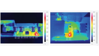
These implementations also reflect very compact designs, with the small magnetics and compact control allowing high implementation density without efficiency tradeoffs.
Figure 4(a) shows an overall end-end 700W design for industrial and medical usage (the PFC stage, which is characterized above) and Figure 4(b) shows the 3kW implementation.

Figure 4(a). 700W Universal Line to 12V Converter in 76mm x 127mm (3”x5”) footprint

Figure 4(b). 3kW PFC Stage in 1U/80mm format
Drive and Control
Recent developments allow driving of the multilevel switches with low component count and at low cost, integrating drive and control into a single “daughter card”. These ICERGi® developments have allowed the inherent advantages of multilevel technologies to be realized in a practical and cost-effective fashion at relevant power levels, typically the 300Wà3kW range as needed for most of the single-phase power factor correction marketplace.
A low-cost commodity ARM-based digital controller works well in control of multilevel converters and is designed for the optimal usage of the driver characteristics. The overall control and drive functionality are captured at a low cost in this component-type “daughter board” as shown in Figure 5. This connects directly to the power MOSFETs and effectively integrates control and drive elements in a 35mm x 26mm card.
Solutions
A key ICERGi “mission” is to make multilevel solutions practical and very cost-effective for use in high-volume AC-DC power conversion.
ICERGi offers:
- Overall control modules – essentially as shown in Figure 5.
- A “Chip Set” for user implementation, along with printed circuit board samples and Gerber layout detail. The chip set comprises the controller chip along with 8 driver chips, one for each FET in a “4+4” device stack.

Figure 5. Control card and interfaces
The ICERGi devices are priced such that high efficiency using multilevel silicon is considerably more cost-effective than using wide bandgap approaches.
A particular point of comparison relates to a multilevel implementation vs the established interleaving approaches, an example of which is in Figure 6.

Figure 6. Showing the established interleaved-boost implementation
If one takes, for example, a two-phase interleaving design, there are two magnetics, each of which has the full volt-seconds. In the multilevel approach, the volt-seconds effectively cancel before the magnetic element – and thus the magnetic element can be made a lot smaller. And switching in the conventional interleaved approach is at full-frequency and full-voltage. This involves materially greater loss than in the multilevel case, with reduced cell switching frequency and voltage.
The interleaved approach also requires a low-Qrr diode for each phase – again part of the cost equation. Finally – the conventional interleaved approach has an extra diode in the conduction path – adding further to losses. It is thus to be expected that a multilevel solution can be at cost parity or below the cost of an interleaved design, with losses reduced by 50% - typically going from 95% stage efficiency to 97.5% at low line.
Summary
Yes, established, low-cost silicon can achieve better than 99% efficiency in power factor correction usage. Multilevel solutions also have a sustainable advantage in magnetics size and EMI/EMC performance, as well as an expected long-term cost advantage over WBG (SiC and GaN) devices.
About the Author
Garry Tomlins holds a Bachelor's Degree in Applied Physics at the University of London. He currently works as the Director at ICERGi, focusing on helping place ICERGi's innovative low-cost power technology.
Trong Tue Vu holds a Ph.D. in Electronics Engineering at Maynooth University, a Master's Degree in Electrical, Electronics and Communications Engineering at Dublin City University, and a Bachelor's Degree in Electrical, Electronics and Communications Engineering at Ho Chi Minh City University of Technology. Trong Tue Vu is currently the CEO of ICERGi Ltd. since January 2018.
This article originally appeared in the Bodo’s Power Systems magazine.